How to design the PCB layer to achieve the best EMC effect?
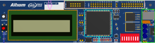
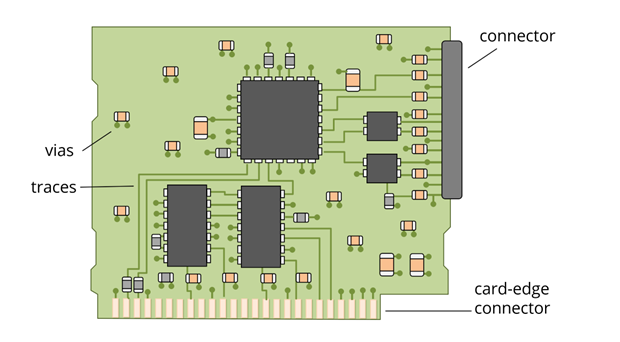
In the EMC design of PCB, the first thing involved is the layer setting; the number of layers of a single board is composed of the number of power supply layers, the number of ground layers and the number of signal layers; in the EMC design of the product, in addition to the selection of components and circuit design, good PCB design is also a very important factor.
The key to the EMC design of PCB is to reduce the return area as much as possible and let the return path flow in the direction we designed. The design of the layer is the foundation of PCB. How to do a good job in the design of the PCB layer to achieve the best EMC effect of PCB?

1.Design ideas of PCB layer
The core of PCB stacking EMC planning and design ideas is to reasonably plan the signal return path, minimize the return area of the signal from the single board mirror layer as much as possible, so that the magnetic flux is canceled or minimized.
Single board mirror layer
The mirror layer is a complete copper-clad plane layer (power layer, ground layer) adjacent to the signal layer inside the PCB. It has the following main functions:
(1) Reduce return noise: The mirror layer can provide a low-impedance path for the signal layer return, especially when there is a large current flowing in the power distribution system, the role of the mirror layer is more obvious.
(2) Reduce EMI: The presence of the mirror layer reduces the area of the closed loop formed by the signal and the return current, reducing EMI;
(3) Reduce crosstalk: It helps to control the crosstalk problem between signal traces in high-speed digital circuits. By changing the height of the signal line from the mirror layer, the crosstalk between signal lines can be controlled. The smaller the height, the smaller the crosstalk;
(4) Impedance control to prevent signal reflection.
Selection of mirror layer
(1) Both the power and ground planes can be used as reference planes and have a certain shielding effect on internal routing;
(2) Relatively speaking, the power plane has a higher characteristic impedance and a larger potential difference with the reference level. At the same time, the high-frequency interference on the power plane is relatively large;
(3) From the perspective of shielding, the ground plane is generally grounded and used as a reference point for the reference level. Its shielding effect is far better than that of the power plane;
(4) When selecting a reference plane, the ground plane should be preferred, and the power plane should be secondary.
II. Principle of flux cancellation
According to Maxwell’s equations, all electrical and magnetic effects between discrete charged bodies or currents are transmitted through the intermediate region between them, regardless of whether the intermediate region is a vacuum or a solid substance. In PCB, magnetic flux always propagates in the transmission line. If the RF return path is parallel to its corresponding signal path, the magnetic flux on the return path is in opposite directions to the magnetic flux on the signal path. At this time, they are superimposed on each other, and the effect of flux cancellation is obtained.
3.The essence of flux cancellation
The essence of flux cancellation is the control of the signal return path. The specific schematic diagram is as follows:
4.The right-hand rule explains the flux cancellation effect
How to use the right-hand rule to explain the flux cancellation effect when the signal layer is adjacent to the ground layer? The explanation is as follows:
(1) When a current flows through a conductor, a magnetic field will be generated around the conductor. The direction of the magnetic field is determined by the right-hand rule.
(2) When there are two conductors close to each other and parallel, as shown in the figure below, the current of one conductor flows outward and the current of the other conductor flows inward. If the currents flowing through the two conductors are the signal current and its return current, respectively, then the two currents are equal in magnitude and opposite in direction, so their magnetic fields are also equal in magnitude and opposite in direction, so they can cancel each other out.

Design examples of five- and six-layer boards
For six-layer boards, plan 3 is preferred
Analysis:
(1) Since the signal layer is adjacent to the return reference plane, and S1, S2, and S3 are adjacent to the ground plane, there is the best flux cancellation effect. The wiring layer S2 is preferred, followed by S3 and S1.
(2) The power plane is adjacent to the GND plane, and the distance between the planes is very small, which has the best flux cancellation effect and low power plane impedance.
(3) The main power supply and its corresponding ground are arranged on layers 4 and 5. When setting the layer thickness, increase the spacing between S2-P and reduce the spacing between P-G2 (correspondingly reduce the spacing between G1-S2 layers) to reduce the impedance of the power plane and reduce the impact of the power supply on S2.
For six-layer boards, alternative plan 4
Analysis:
For occasions with high requirements for local and small amounts of signals, plan 4 is more suitable than plan 3, and it can provide an excellent wiring layer S2.
Worst EMC effect, Scheme 2
Analysis:
In this structure, S1 and S2 are adjacent, S3 and S4 are adjacent, and S3 and S4 are not adjacent to the ground plane, so the magnetic flux cancellation effect is poor.
Summary
Specific principles of PCB layer design:
(1) There is a complete ground plane (shielding) under the component surface and welding surface;
(2) Try to avoid two signal layers being directly adjacent to each other;
(3) All signal layers should be adjacent to the ground plane as much as possible.