How to Design with Capacitive Digital Isolators
Currently, safety regulations regarding the use and design of electronic devices have made galvanic isolators a necessity in almost all data acquisition and transmission systems. One way to protect the low-voltage circuits of the control system from the potential high voltage damage of sensor and actuator components in the electric field is to use digital isolators.
The purpose of this article is to tell you how to simplify the design of isolated systems. In addition to describing the basic functions of capacitive digital isolators, the article details how to install isolators in the signal path, and provides some valuable references for successful circuit board design.
Basic Functions of Capacitive Digital Isolators
Figure 1 shows a simplified block diagram of a capacitive digital isolator, which consists of a high-speed signal path and a low-speed signal path. The high-speed path (blue part) transmits signals from 100kbps to 150Mbps, while the low-speed path (orange part) transmits signals below 100kbps to dc.
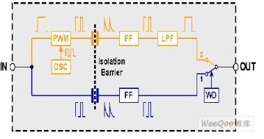
Figure 1 Simplified Block Diagram of Capacitive Digital Isolator
The high-speed signal processed in the path shown in the blue part is divided into multiple fast transient pulse groups by the capacitive isolation barrier. The subsequent flip-flop (FF) converts these transient pulse groups into pulses with waveforms and phases that match the input signal. The internal watchdog (WD) checks the periodicity of the high-speed signal edges. In the case of low-frequency input signals, the duration between consecutive signal edges exceeds the watchdog window. This forces the watchdog to change the output switch position from the high-speed path (position 1) to the low-speed path (position 2).
The low-speed path has several more functional elements than the high-speed path. Because the low-frequency input signal requires an isolation barrier that prohibits the use of large capacitors, the input signal is used to pulse-width modulate (PWM) the carrier frequency of the internal oscillator (OSC). This creates a very high frequency that can pass the capacitive barrier. Since the input is modulated, a low-pass filter (LPF) must be used to remove the high-frequency carrier before the actual data is transmitted to the output.
Where to Install in the Signal Chain
Digital isolators are available in single, dual, triple, and quad channel devices that can operate in both unidirectional and bidirectional modes. They all share the following characteristics:
- Not compliant with any particular interface standard;
- Use 3V/5V logic switch technology
- Designed to electrically isolate digital, single-ended (SE) data lines
While the last point may seem like a design limitation, Figure 2 shows how to isolate a wide variety of interfaces, including low voltage SPI, high voltage RS232, differential USB, and differential CAN/RS485.
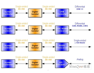
Figure 2 Digital isolators must be installed in the single-ended portion of the isolated interface
One thing that all interfaces have in common is that the digital isolator must be installed in the single-ended 3V/5V portion of the isolated interface.
Because digital isolators have rise and fall times of 1 to 2ns, they are often susceptible to signal reflections in the case of long signal traces, where the characteristic impedance does not match the source impedance of the isolator output. Therefore, we recommend installing an isolator close to its corresponding data receiving device and data source (such as controllers, drivers, receivers, and transceivers). If this is not possible in the design, then controlled impedance transmission lines must be used.
PCB Design Guidelines
For digital circuit boards, standard FR-4 epoxy glass is used as the PCB material. This is because compared with cheaper materials, it not only meets UL94-V0 requirements, but also has lower high-frequency dielectric losses, lower moisture absorption, greater strength/hardness, and higher flame retardancy.
To achieve a low electromagnetic interference (EMI) PCB design, here is a minimum of four layers (see Figure 3), which are from top to bottom: high-speed signal layer, ground layer, power layer, and low-frequency signal layer.

Figure 3 Recommended four-layer board stackup
Placing high-speed traces on the top layer provides a clear connection for the isolator and its corresponding driver. High-speed traces should be short and avoid the use of vias to ensure that the high-speed trace inductance is minimized.
Place a balanced ground plane just after the high-speed signal layer to ensure strong electrical coupling between the ground plane and the signal traces. This creates a controlled impedance for the transmission line interconnects, while also greatly reducing EMI. Ultimately, the balanced ground plane provides a very good low-inductance path for return currents.
Place the power plane below the ground plane. The two reference planes form an additional high-frequency bypass capacitor of about 100pF/in2.
Route low-speed control signals on the bottom layer. These signal links have enough margin to withstand interruptions caused by vias, allowing for greater flexibility.
A controlled impedance transmission line is a trace whose characteristic impedance, Z0, is always controlled by its geometric characteristics. For trace lengths greater than 15mm (tr=1ns) and 30mm (tr=2ns), the trace impedance must be matched to the isolator output impedance Z0″rO (as shown in Figure 4) to minimize signal reflections. This is called source impedance matching.
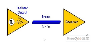
Figure 4 Source impedance matching: Z0 ” rO
The dynamic output impedance of the isolator, r0, can be obtained by approximating the linear portion of the voltage-current output characteristic listed in the isolator data sheet. Generally speaking, the standard output impedance is about 70Ω. Therefore, for a standard 2-ounce copper plated wire and FR-4 with a dielectric of 4.5, a trace geometry of 8mm wide and 10mm long on the ground plane will produce the required 70Ω characteristic impedance.
Routing Guidelines
It is recommended to follow several key routing guidelines to maintain signal integrity and low EMI.
To reduce crosstalk to less than 10%, keep the signal trace three times the distance from the high-speed signal layer to the ground layer (d=3h). The return current density under the signal trace follows the function 1/[1+(d/h)2], so its density is very low at the point where d>3h, thus avoiding large crosstalk in adjacent traces (see Figure 5).
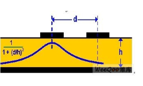
Figure 5 Minimizing crosstalk with d = 3h
Using 45o trace bends (or chamfered bends) instead of 90o bends maintains effective trace impedance and avoids signal reflections.
To achieve operation in noisy environments, connect the idle enable input of the isolator to a suitable reference plane through a resistor (1kΩ to 10kΩ). Connect the active-high, high-enable input to the power plane, and the active-low input to the ground plane.
Avoid changing layers with fast signal traces as via inductance increases the inductance of the signal path.
Use short trace lengths between the isolator and surrounding circuits to avoid noise introduction. Digital isolators are often accompanied by an isolated DC/DC converter that provides power across the isolation layer. Since the single-ended transmission signal of the isolator is too sensitive to noise injection, the switching noise of the adjacent DC/DC converter can be easily introduced by the long signal traces.
Place large-capacity capacitors (such as 10μF) close to the power supply such as the regulator, or where the power supply enters the PCB.
Install small-capacity 0.1μF or 0.01μF bypass capacitors on the device by connecting the power supply terminal of the capacitor directly to the power supply terminal of the device and then connecting to the Vcc layer through vias. Connect the ground terminal of the capacitor to the ground plane through several vias (see Figure 6).
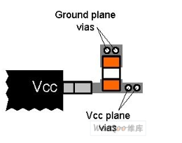
Figure 6 Connect bypass capacitors directly to the Vcc terminal
Use multiple vias to connect bypass capacitors and other protection devices (such as transient voltage suppressors and Zener diodes) to minimize the via inductance of the ground connection.
Summary
Although there is a lot of information on PCB design, this article focuses on some suggestions for digital isolator board design. Following these suggestions will help you complete a board design that meets EMC standards in the shortest time.