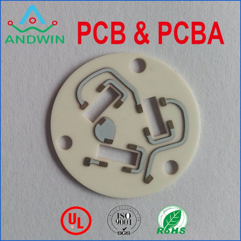
How to Do Micro PCB Design and Fabrication
Here are some tips to help you understand how to do micro PCB design and fabrication.
Today, the reduction in size of basic circuit boards will allow designers to reduce the size of their PCBs by half, or down to a quarter of the original size. Very fine lines that were previously unavailable to designers will now become mainstream, and the original minimum line width of 75 microns (3mils) is gradually reduced to 30 microns (1.2mils) or less.
New design rules are needed for smaller traces and vias because the manufacturing methods of PCB circuit boards are completely different and advanced. Microelectronic PCB circuit manufacturers cannot reliably manufacture lines below 75 microns using the standard old dry film, flat plate and etching processes. Photolithography is the method of choice to produce these very fine lines and spaces. The move to smaller line widths may catch off guard quite a few “stuck in the mud” old-fashioned printed circuit manufacturers who now don’t even offer 3mils. To remain competitive in the near future, PCB shops will need to offer at least 50 micron lines and spaces, and even as low as 30 microns.
Micro PCB Manufacturer Groups
Manufacturers of fine microcircuits fall into four groups. The first group is mainly Asian, developing unique fine-line processes for cell phones or iPods that lay out 40-50 micron traces. The second group is a limited number of R&D companies that only make small quantities of very specialized circuits with fine lines below 40 microns on Kapton, which has high costs, lead times of up to three months, and small production volumes.
The third group is the fastest expanding business of medium-sized PCB circuit companies that offer smaller production quantities with line widths of 75 to 40 microns, producing thousands in a few weeks. Finally, the fourth group is normal fine-line PCB production with dimensions of 125 to 75 microns, with high-volume production and many players. We place ourselves in the fifth group. We have developed a new manufacturing technology that is capable of forming 30 micron lines and spaces on FR4 or Kapton.
As the microelectronics business expands and more and more PCB circuit companies discover the technology necessary to manufacture very fine lines of 40 microns and below, circuit designers will need to become familiar with the new design rules and the advantages and disadvantages of microcircuit manufacturing.
How to Design a Micro PCB
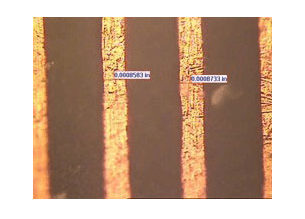
For obvious reasons, very fine 30 micron lines cannot use normal 1 oz copper. When we reduce the line width, we must reduce the thickness. At Sierra Circuits, we have made 25 micron lines using 18 micron thick copper, but that is about the upper limit. Thinner copper traces should not be a problem unless your design uses higher currents, in which case a particular trace can be made wider to handle the higher currents. A 30 micron line is robust and reliable, however, it does not suffer from too many physical limitations that can be all but eliminated by using a typical solder mask.
Thin lines may worry many designers, however, who need to take the 200 micron wide traces they are currently starting with and reduce them to the 25 to 13 micron aluminum or gold round wires that connect the chip to the chip carrier. The thin lines are encapsulated in multiple layers of inner layers or by solder mask, which means they are virtually locked in. New methods of attaching copper to the board surface have been developed and these are used to improve the overall adhesion of micro traces to the surface.
Some of the first micro designs had a large fillet from the 30 micron trace to the pad. Over time, it proved to be unnecessary. Routing the trace directly to the pad is very robust and reliable. The extra fillet just proved to increase image writing time and cost.
Small vias: There is a physical limit to how small a micro via can be. Below 50 microns (2mils), the plating solution will not properly plate the hole walls, resulting in poor via quality. Our lasers can drill holes as small as 20 microns, but we cannot plate them. The thickness of the laminate controls the minimum diameter of the via, and for plated micro vias, there is an upper limit of 2:1.
For example, a 3mil micro via is limited to a 6mil thick laminate in terms of plating. There is also a limit to how deep our Yag lasers can drill a via. As the diameter decreases, the ability to penetrate the laminate to form a clean hole decreases. A 3mil via is limited to 4 to 5mils in depth in FR4 and 6 to 7mils in glass-free laminates used in HDI applications. Everything about microvias is not necessarily bad. A microvia may not be able to be as small as a trace, but we can add sweetener to the pot because the annular ring around the microvia will be noticeably smaller.
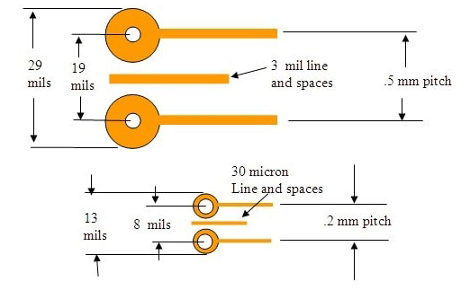
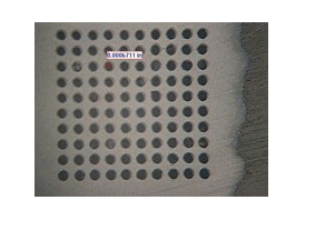
When we produced our first micro PCB, the first thing we noticed was that the via was centered in the pad. The design used a 9mil pad and a 3mil via, which is tight for traditional printed circuit engineering. New more precise laser manufacturing methods will allow pads as small as 5mils and vias as small as 3mils, saving a lot of board area.
(9mils pad and 3mil via with 40 micron line)
Using new microcircuit design techniques instead of conventional printed circuit techniques can save a lot of space. Today, the optimal pitch for a typical 75 micron line width is about .5mm, giving a 75 micron (3mil) via with a 75 micron line and a 250 micron (10mil) pad. With 225 microns (9mils) between pads, and only a 75 micron line allowed between pads, this minimum spec is difficult for most shops to meet.
Micro PCB Design Guidelines
Microcircuit technology utilizing 3mils vias, 5mils, 30 micron lines, and 30 micron spaces produces a 0.2mm pitch layout. Microcircuit technology reduces the area used by a factor of five compared to a standard 3mil PCB layout. In a future article, we will discuss the idea of reducing the required component area. However, even with the same components, simply switching to 30 micron lines and smaller pads will significantly reduce board area. When routing, use the same techniques, but try to angle the lines when making turns instead of using 90 degree turns. An angled line at a corner distributes the corner stress over a larger area.

1.Microvias
When utilizing HDI technology layers added on top of multilayer boards or as all HDI multilayers, microvias can be used to connect between thin layers. Vias can be drilled to 5.9mils diameter (up to 60mils), or laser drilled to 2-3mils diameter, but only on 2-4mils thick HDI laminates. Keep in mind that drilled holes have a large drift compared to laser created holes, which limits pad to hole size. For drilled holes, use 12 mil pads and 6 mil holes, while for laser drilled microvias, 5 mil pads can be used with 3 mil vias.
2.Hole Size
Although it may seem obvious, it is worth reiterating: every element of traditional PCB design needs to be adjusted to accommodate the smaller micro dimensions. This can be a challenge for PCB layout engineers familiar with traditional PCB design. The most common mistake we see in this area is oversized holes. In fact, micro PCB designs should have laser micro vias to interconnect between substrate layers. If the holes in the design are too large (which they usually are), it will result in a suboptimal or even failed micro PCB.
This again goes back to the importance of working with the right micro PCB manufacturer. When a PCB company is your partner, you will have an expert to turn to for help at every step of the PCB process to ensure that your micro PCB design meets all the required requirements.
3.Copper Thickness
Normal 3mils fine line circuits are 1 ounce copper, and microcircuits use oz per 30 micron width. Normal pattern plating is used to make microcircuits, which means that the traces do not have to lead out of the circuit to the plated bus, the pattern plating connects to the entire circuit, and the wire bond plating is chemical or electrical.
4.Reliability
Most normal printed circuit boards can be used for HDI or microcircuits, but both have limitations. Micro single-sided and double-sided circuits can be made of rigid FR4 type laminates, but they must be thin to allow for micro vias.
5.Electrical Testing
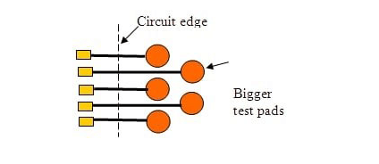
Currently, the lower limit for flying probe or even rigid probe (bed of nails) technology is 2-3mils. We expect this to decrease over time as smaller platforms are needed as necessary. If your microcircuit has small points (e.g. edge strip connectors), it is wise to extend the lines outside the circuit to 3-4 mil pads.
6.Solder Mask
Unfortunately, the imaging technology that allows us to make 30 micron lines has not yet been transferred to solder mask. 75 micron position accuracy as well as image resolution is still the limit.
7.Identification Marking
Typical screen printing image accuracy is too large for microcircuits. Sierra Proto uses a very fine inkjet printer, which results in very small identification mark resolution.
8.Security Marking
A very small individual barcode can be imaged into the solder mask to properly identify the printed circuit board. The barcode is so small that it is almost invisible to the human eye.
8-micron security barcode
15-micron production line development
9.Final finish
A normal printed circuit board can be used. Most microcircuits use soft gold, immersion tin, or silver to which wires can be bonded.
10.Understand the manufacturer’s capabilities
This is by far the most important step when undertaking a micro PCB design, regardless of the specific application or type of microelectronics you are developing. Basic skills are extremely important at any time when designing a PCB. However, understanding their capabilities and services is especially important for micro PCBs. This is critical for a company that has never worked on a micro PCB design, or has never worked with a designated PCB manufacturing company to develop such a product. The reason is simple: micro PCB manufacturing capabilities vary greatly from one PCB manufacturer to another. In fact, micro PCBs are still fairly new and complex enough that many PCB manufacturers will offer limited microelectronics capabilities or support. To prove a micro PCB design successful, you need to ensure that the manufacturer can meet your basic requirements. Remember, your design needs to meet their guidelines. If you incorporate elements into your design that the manufacturer cannot meet, rework will be required. This will cause delays, slowing down turnaround time and speed to market.