How to draw GND on pcb
In the circuit principle design stage, in order to reduce mutual interference between circuits, engineers generally introduce different GND ground wires as 0V reference points for different functional circuits to form different current loops.
1.Classification of GND ground wires

2.A detailed study of the principle of GND
How can a ground wire GND have so many distinctions, and how can a simple circuit problem be so complicated? Why is it necessary to introduce so many subdivided GND ground wire functions? Engineers generally simply name this type of GND ground wire design problem as GND, and do not distinguish it during the schematic design process, which makes it difficult to effectively identify the GND ground wires of different circuit functions during PCB wiring, and simply connect all GND ground wires together. Although this operation is simple, it will lead to a series of problems:
· Signal crosstalk. If the ground wires GND of different functions are directly connected together, the high-power circuit will affect the 0V reference point GND of the low-power circuit through the ground wire GND, thereby generating crosstalk between different circuit signals.
· Signal accuracy. The core indicator of analog circuit assessment is signal accuracy. Without accuracy, the analog circuit will lose its original functional significance. Since the ground wire CGND of the AC power supply is a sine wave, it fluctuates up and down periodically, and its voltage also fluctuates up and down, not like the DC ground wire GND, which always remains at 0V. When the ground wires GND of different circuits are connected together, the periodically changing AC ground wire CGND will drive the ground wire AGND of the analog circuit to change, thus affecting the voltage accuracy value of the analog signal.
· EMC experiment. The weaker the signal, the weaker the external electromagnetic radiation EMC; the stronger the signal, the stronger the external electromagnetic radiation EMC. If the ground wires GND of different circuits are connected together, the ground wire GND of the circuit with strong signal directly interferes with the ground wire GND of the circuit with weak signal. As a result, the electromagnetic radiation EMC with weak signal becomes the signal source of strong external electromagnetic radiation, which increases the difficulty of EMC experiment of circuit processing.
· Circuit reliability. The fewer signal connection parts between circuit systems, the stronger the ability of circuit to operate independently; the more signal connection parts, the weaker the ability of circuit to operate independently. Imagine that if two circuit systems A and B have no intersection, the function of circuit system A cannot affect the normal operation of circuit system B, and the function of circuit system B cannot affect the normal operation of circuit system A. If the ground wires of circuits with different functions are connected together in the circuit system, it is equivalent to adding a link of interference between circuits, which reduces the reliability of circuit operation.
3.Teach you to draw “GND” step by step
The importance of “GND” on a PCB board is no less than that of water to the human body. How to draw “GND” well? Just pay attention to the following points.
Do a good job of partitioning “GND”
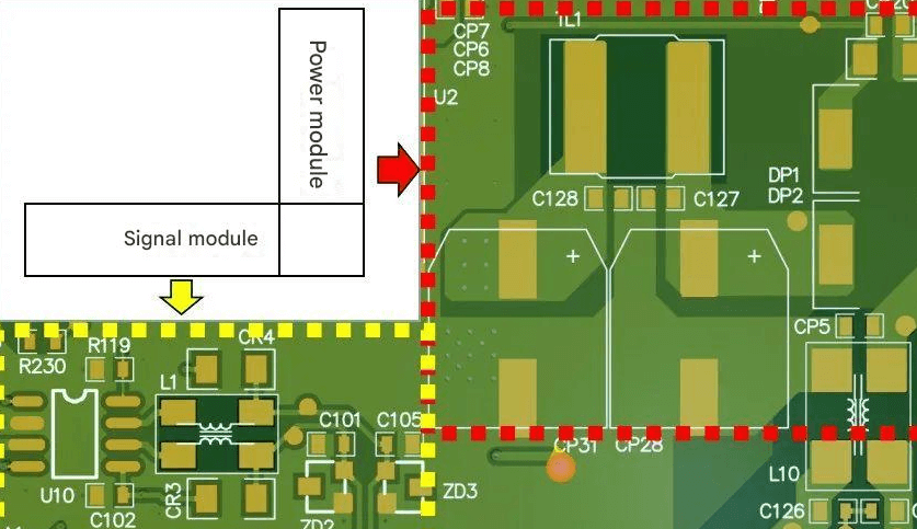
On the PCB board, different module functions will be distributed in different positions, and the “GND” requirements of the corresponding modules will also be different. The figure below is a drawing board where the power ground and the signal ground conflict. In this circuit, the actual function of the power supply GND is “negative power supply” rather than “0V reference ground”, while the actual function of the signal part GND is “0V reference ground”. In this case, the unclean power ground causes interference to the signal part! There are two ways to deal with this situation:
- Separate the ground of the signal part from the GND of the power supply part, and do not connect directly;
- Hollow out the GND of the signal part. If power is needed, use routing to supply power
Don’t step over “GND”
There are also some GNDs that should be complete for a module due to the structure, but are divided into multiple areas of stepped GND by other routings. For example, as shown in the PCB circuit below, the negative pole of the power input directly becomes “GND” after being connected to the PCB board, which is position ①. In the direction of the power module, ① and ② are separated by the signal line; ② and ③ are separated by the 5V output; and ③ and ④ are separated by the chip enable. Although the GND of this layout is connected when measured with a multimeter, it is unreasonable from the order of the wiring on the schematic diagram and the “ground impedance” under high frequency conditions. Especially as the power module is one of the core issues of EMC, the ground layout must be complete on the same layer!
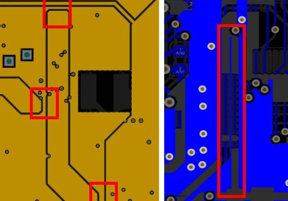
Reject the “GND” with a small waist
When copper or grounding the entire PCB board, there are often some places where “GND” and “GND” appear “small waist” due to wiring or vias in other positions! For example, in the two pictures below, the left is the “small waist” type GND, and the right is the “pig tail” type GND. These two styles of GND are not a good layout for EMI and EMS! The “slim waist” type GND can be widened, or copper laying is prohibited in too narrow areas, while the “pig tail” type GND is best not to be cut off. If it is required for other functions, more vias can be added to ensure that the grounding is OK.
The “GND” on the PCB board requires repeated inspections by engineers and consideration of the overall layout. Don’t be perfunctory for convenience, and don’t ground for the sake of grounding! When laying copper “GND”, be sure to distinguish whether the GND of each part can be laid through, whether there is “unreasonable” GND between densely packed traces, and the actual role of “GND” in each area!