How to Ensure Correct Layer Stackup in PCB Design
Introduction
Printed Circuit Board (PCB) layer stackup is a critical aspect of modern electronic design that directly impacts signal integrity, power delivery, electromagnetic compatibility (EMC), and manufacturability. As PCBs become more complex with higher layer counts and faster signal speeds, proper stackup design has evolved from being merely important to absolutely essential. This article provides a comprehensive guide on how to ensure correct layer stackup in PCB design, covering fundamental principles, material selection, stackup configuration strategies, verification methods, and common pitfalls to avoid.
Understanding PCB Layer Stackup Fundamentals
Definition and Importance
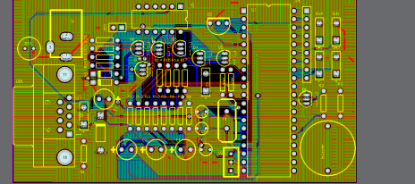
PCB layer stackup refers to the arrangement of copper layers and insulating dielectric materials that make up a multilayer printed circuit board. A well-designed stackup:
- Maintains signal integrity by controlling impedance
- Provides stable power distribution
- Minimizes electromagnetic interference (EMI)
- Ensures mechanical stability
- Facilitates efficient manufacturing
Key Stackup Parameters
Several critical parameters define a PCB stackup:
- Layer count: Determined by circuit complexity and routing requirements
- Dielectric materials: Typically FR-4, but high-speed designs may use specialized materials
- Copper weights: Expressed in ounces per square foot (e.g., 0.5 oz, 1 oz, 2 oz)
- Dielectric thickness: Distance between adjacent copper layers
- Impedance targets: Critical for high-speed signals (typically 50Ω single-ended, 100Ω differential)

Step-by-Step Process for Correct Stackup Design
1. Define Design Requirements
Begin by gathering all necessary design requirements:
- Number of signal layers needed
- Power delivery requirements
- Signal speed and integrity considerations
- EMI/EMC requirements
- Mechanical constraints (board thickness, flex requirements)
- Thermal management needs
- Cost targets
2. Select Appropriate Materials
Choose materials based on electrical, thermal, and mechanical requirements:
- Standard FR-4: Cost-effective for most applications
- High-speed laminates: Lower dielectric loss for RF/high-speed designs
- Flex materials: For flexible or rigid-flex designs
- Metal cores: For power electronics or high thermal dissipation
Consider dielectric constant (Dk), dissipation factor (Df), thermal conductivity, and glass transition temperature (Tg).
3. Determine Layer Arrangement
Follow these fundamental rules for layer arrangement:
- Signal layers: Should be adjacent to ground planes for controlled impedance
- Power planes: Should be paired with adjacent ground planes to form decoupling capacitance
- High-speed signals: Route on inner layers between ground planes for shielding
- Sensitive analog signals: Keep separate from digital signals with ground isolation
A typical 4-layer stackup might be:
- Top (signal)
- Ground
- Power
- Bottom (signal)
For 6-layer boards:
- Top (signal)
- Ground
- Signal
- Signal
- Power
- Bottom (signal)
4. Calculate Impedance and Thickness
Use field solver tools or industry-standard formulas to:
- Calculate required dielectric thicknesses to achieve target impedances
- Determine trace widths for microstrip and stripline configurations
- Account for copper roughness effects at high frequencies
Maintain consistency in impedance throughout the signal path, including through vias and connectors.
5. Symmetry and Balance
Design stackups to be symmetric about the center layer to prevent warping during manufacturing:
- Balance copper distribution across layers
- Mirror material thicknesses above and below the center
- Consider thermal expansion coefficients
6. Document the Stackup
Create a detailed stackup drawing including:
- Layer sequence and purpose
- Material types and suppliers
- Dielectric thicknesses
- Copper weights
- Finished board thickness
- Impedance targets and calculated trace widths
Verification and Validation Methods
1. Pre-manufacturing Verification
Before sending designs to fabrication:
- Review with fabricator: Ensure the stackup is manufacturable
- Signal integrity analysis: Use simulation tools to verify performance
- Cross-section review: Check for proper symmetry and material distribution
2. Post-manufacturing Validation
After receiving prototypes:
- Impedance testing: Use TDR (Time Domain Reflectometry) to measure actual impedances
- Cross-section analysis: Verify layer thicknesses and material consistency
- Signal integrity measurements: Validate high-speed performance
Common Stackup Mistakes and How to Avoid Them
1. Improper Layer Sequencing
Mistake: Placing signal layers adjacent to each other without reference planes
Solution: Always sandwich signal layers between ground/power planes
2. Ignoring Manufacturability
Mistake: Specifying exotic materials or tight tolerances without consulting fabricator
Solution: Discuss stackup with fabricator early in design process
3. Inadequate Power Delivery
Mistake: Insufficient power planes or improper distribution
Solution: Analyze power requirements and provide adequate copper for current needs
4. Neglecting Thermal Considerations
Mistake: Not accounting for thermal expansion or heat dissipation
Solution: Include thermal analysis in stackup design, consider thermal vias
5. Overlooking DFM Rules
Mistake: Designing stackups that push fabrication limits unnecessarily
Solution: Follow manufacturer’s Design for Manufacturing (DFM) guidelines
Advanced Stackup Considerations
1. High-Speed Design Techniques
For designs with signals above 1GHz:
- Use low-loss dielectric materials
- Implement buried capacitance layers
- Consider ultra-thin dielectrics for power-ground coupling
- Account for skin effect in copper thickness selection
2. HDI (High Density Interconnect) Stackups
For HDI designs with microvias:
- Plan for sequential lamination steps
- Include laser-drillable dielectric materials
- Manage via stub effects in layer transitions
3. Mixed-Signal Designs
For boards with both analog and digital circuits:
- Implement split ground planes with controlled connections
- Provide separate power domains
- Use shielding layers between sensitive sections
Collaboration with PCB Manufacturers
Effective stackup design requires close collaboration with PCB fabricators:
- Early engagement: Involve fabricator during initial design phases
- Material availability: Verify preferred materials are in stock
- Process capabilities: Understand manufacturer’s limitations on layer counts, thickness tolerances, etc.
- Testing protocols: Agree on measurement and validation methods
Tools for Stackup Design and Analysis
Several software tools assist in proper stackup design:
- Stackup calculators: Polar Instruments Si9000, Altium Layer Stack Manager
- 3D EM field solvers: Ansys HFSS, CST Studio Suite
- Signal integrity tools: Keysight ADS, Cadence Sigrity
- Thermal analysis tools: Mentor Graphics FloTHERM
Conclusion
Proper PCB layer stackup design is both an art and a science that requires careful consideration of electrical, mechanical, and manufacturing requirements. By following systematic design practices, collaborating closely with fabrication partners, and leveraging appropriate analysis tools, designers can create robust stackups that meet performance targets while remaining manufacturable. As board complexities continue to increase with advancing technologies, attention to proper stackup design will remain a critical factor in successful PCB implementation.
Remember that stackup design isn’t a one-time activity—it should be revisited throughout the design process as requirements evolve and new constraints emerge. By making stackup design a priority rather than an afterthought, engineers can avoid costly redesigns and ensure optimal performance of their electronic systems.


