How to Generate a PCB from a Schematic: A Comprehensive Guide
Introduction
The process of transforming an electronic schematic into a functional printed circuit board (PCB) is a fundamental skill for electrical engineers and electronics designers. This conversion bridges the gap between theoretical circuit design and practical implementation. While modern electronic design automation (EDA) tools have simplified much of this process, understanding each step remains crucial for creating reliable, manufacturable PCBs.
This 2000-word guide will walk you through the complete workflow from schematic capture to PCB generation, covering essential concepts, best practices, and common pitfalls to avoid.
1. Schematic Design: The Foundation
Before generating a PCB, you must create a complete and accurate schematic diagram:
1.1 Schematic Capture Basics
- Use professional EDA software (Altium Designer, KiCad, Eagle, OrCAD, etc.)
- Create logical representations of all components and their connections
- Organize the schematic hierarchically for complex designs
- Use clear labeling and net names for important signals
1.2 Component Selection
- Choose components with available footprints (or create custom ones)
- Verify electrical parameters match design requirements
- Consider availability and lead times for production
- Account for power ratings and thermal characteristics
1.3 Design Verification
- Run electrical rules checking (ERC) to catch common errors
- Verify all nets are properly connected
- Check for floating pins or unconnected power supplies
- Confirm component values match the bill of materials (BOM)
2. Preparing for PCB Layout
2.1 Component Footprint Assignment
- Match schematic symbols to physical PCB footprints
- Verify pad sizes match component datasheet requirements
- Check mechanical dimensions for proper spacing
- Create custom footprints when necessary
2.2 Design Rules Setup
- Define minimum trace widths based on current requirements
- Set clearance rules for voltage differences
- Configure via sizes and drill requirements
- Establish copper-to-edge spacing (board outline clearance)
2.3 Netlist Generation
- The netlist serves as the bridge between schematic and PCB
- Contains all component connections and properties
- Modern EDA tools typically handle this automatically
- Verify netlist matches schematic before proceeding
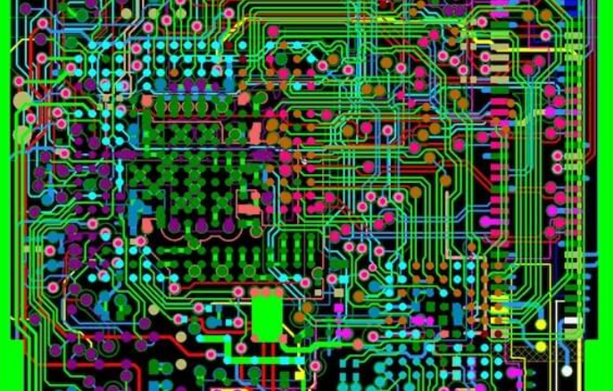
3. PCB Layout Process
3.1 Board Outline Definition
- Set physical dimensions based on enclosure requirements
- Define mounting hole locations
- Consider panelization needs for manufacturing
- Add any required cutouts or special features
3.2 Component Placement
- Start with critical components (connectors, processors, etc.)
- Group related circuits together (power, analog, digital)
- Consider thermal management and heat dissipation
- Follow manufacturer’s recommended layout for sensitive components
- Maintain proper spacing for assembly and rework
3.3 Routing the PCB
3.3.1 Power Distribution
- Use appropriate trace widths for current loads
- Implement power planes when possible
- Consider using a star topology for analog circuits
- Add proper decoupling capacitors near ICs
3.3.2 Signal Routing
- Route critical signals first (clocks, high-speed, sensitive analog)
- Maintain controlled impedance for high-frequency traces
- Avoid sharp angles (use 45° or curved traces)
- Keep differential pairs tightly coupled and length-matched
3.3.3 Layer Stackup Design
- Choose appropriate number of layers for complexity
- Alternate signal and plane layers for better EMI performance
- Define proper dielectric thicknesses for impedance control
- Consider manufacturing capabilities and costs
3.4 Design Rule Checking (DRC)
- Run DRC frequently during layout process
- Verify all constraints are met (spacing, widths, etc.)
- Check for unconnected nets or incomplete routes
- Validate manufacturing constraints (min hole size, etc.)
4. Finalizing the PCB Design
4.1 Silkscreen and Documentation
- Add clear component designators and polarity markers
- Include version numbers and copyright information
- Add test points for debugging and verification
- Consider assembly markings and identifiers
4.2 Copper Pour and Plane Connections
- Implement ground planes for better EMI performance
- Use proper thermal relief connections for components
- Balance copper distribution to prevent warping
- Consider split planes for mixed-signal designs
4.3 Design Verification
- Perform signal integrity analysis for critical traces
- Run power distribution network (PDN) analysis
- Check for potential EMI/EMC issues
- Verify manufacturability with your PCB fabricator
5. Generating Manufacturing Files
5.1 Gerber File Generation
- Export all required layers (copper, silkscreen, solder mask)
- Include drill files (Excellon format typically)
- Generate board outline (typically in Gerber or DXF)
- Verify files using a Gerber viewer before submission
5.2 Bill of Materials (BOM)
- Create complete component list with references
- Include manufacturer part numbers and quantities
- Specify alternatives where available
- Add any special assembly instructions
5.3 Assembly Drawings
- Provide component placement diagrams
- Include any special orientation requirements
- Specify solder paste requirements (for SMD)
- Add mechanical drawings if needed
6. Advanced Considerations
6.1 High-Speed Design Techniques
- Implement proper termination strategies
- Use length matching for parallel buses
- Consider via stitching for better return paths
- Apply appropriate stackup for signal integrity
6.2 Mixed-Signal Layout
- Implement proper grounding schemes
- Partition analog and digital sections
- Use moats or splits when necessary
- Pay attention to sensitive analog routing
6.3 Design for Manufacturing (DFM)
- Follow fabricator’s capability guidelines
- Consider panelization for small boards
- Add fiducial markers for automated assembly
- Include test coupons when required
7. Common Mistakes to Avoid
- Incomplete ERC/DRC: Skipping design rule checks leads to manufacturing issues
- Improper Footprints: Wrong pad sizes or spacing cause assembly problems
- Inadequate Power Distribution: Undersized traces cause voltage drops
- Poor Component Placement: Leads to routing difficulties and signal issues
- Ignoring Thermal Considerations: Overheating reduces reliability
- Insufficient Clearance: Violates safety standards or causes shorts
- Missing Manufacturing Notes: Results in incorrect board fabrication
Conclusion
Generating a PCB from a schematic is a multi-stage process that requires attention to both electrical and physical design considerations. By methodically progressing from schematic capture through final manufacturing file generation, designers can create PCBs that are both electrically sound and manufacturable. Modern EDA tools have automated many aspects of this process, but engineering judgment remains essential for creating optimal designs.
Remember that PCB design is often iterative—be prepared to make adjustments as you encounter routing challenges or identify opportunities for improvement. With practice and attention to detail, the process of converting schematics to functional PCBs will become increasingly efficient and reliable.
As you gain experience, you’ll develop intuition for component placement, routing strategies, and design tradeoffs. Always keep learning from each design, and don’t hesitate to consult with PCB manufacturers early in the process to ensure your designs can be reliably produced at scale.