How to Handle PCB Solderability Issues: Comprehensive Solutions for Poor Solder Wetting
Introduction to PCB Solderability Problems
Printed Circuit Board (PCB) assembly relies heavily on the ability of solder to properly wet and adhere to component leads and copper pads. When PCB surfaces fail to accept solder adequately – a condition commonly referred to as “poor solder wetting” or “PCB not taking solder” – it can lead to significant manufacturing defects, reliability issues, and increased production costs.
Solderability problems manifest in various ways: solder may bead up instead of spreading evenly, leave exposed areas on pads, or fail to form proper intermetallic bonds. These issues can occur during hand soldering, wave soldering, or reflow processes. Understanding the root causes and implementing appropriate solutions is essential for maintaining high-quality PCB production.
This comprehensive guide examines the primary causes of poor solder wetting on PCBs and provides detailed, actionable solutions for each scenario.
Primary Causes of Poor Solder Wetting on PCBs
1. Surface Oxidation and Contamination
Copper Oxidation:
Exposed copper surfaces rapidly form oxide layers when exposed to air. While fresh copper has excellent solderability, copper oxide (Cu₂O and CuO) forms quickly and creates a barrier that prevents proper solder wetting. The oxidation process accelerates with:
- High humidity environments
- Elevated temperatures
- Exposure to corrosive chemicals
Organic Contamination:
Various contaminants can compromise solderability:
- Finger oils from improper handling
- Residual flux from previous processes
- Dust and airborne particles
- Manufacturing residues (lubricants, release agents)
Metallic Contamination:
Some metals like aluminum or heavy metals can transfer onto PCB surfaces during handling, creating solderability barriers.
2. Improper Surface Finishes
The choice and quality of PCB surface finish significantly impacts solderability:
HASL (Hot Air Solder Leveling) Issues:
- Inconsistent thickness
- Oxidized solder surfaces
- Thermal damage from multiple passes
ENIG (Electroless Nickel Immersion Gold) Problems:
- Black pad syndrome (nickel corrosion)
- Excessive gold thickness (>0.15μm can cause embrittlement)
- Poor nickel activation
OSP (Organic Solderability Preservative) Limitations:
- Limited shelf life (typically 6-12 months)
- Degradation during multiple thermal cycles
- Sensitivity to handling
Immersion Silver/Tin Concerns:
- Silver tarnishing
- Tin whisker formation
- Thickness variations
3. Inadequate Soldering Process Parameters
Even with properly prepared surfaces, incorrect soldering parameters can cause wetting issues:
Temperature Problems:
- Insufficient soldering temperature (solder doesn’t melt properly)
- Excessive temperature (flux burns off too quickly)
- Uneven heating (component leads vs. pads)
Time Factors:
- Dwell time too short (incomplete wetting)
- Excessive time (flux depletion, oxidation)
Flux Issues:
- Inadequate flux activity for the application
- Insufficient flux quantity
- Wrong flux chemistry (water-based vs. rosin-based)
Comprehensive Solutions for PCB Solderability Issues
1. Surface Preparation and Cleaning Techniques
Mechanical Cleaning Methods:
- Abrasive cleaning: Use fiberglass pens or very fine abrasives (600+ grit) for spot cleaning
- Micro-etching: Sulfuric acid/hydrogen peroxide solutions remove thin oxide layers
- Brushing: Nylon brushes with cleaning solutions for overall surface preparation
Chemical Cleaning Processes:
- Alkaline cleaners: Effective for organic contamination removal
- Acid treatments: Mild acid solutions (5-10% sulfuric or hydrochloric) for oxide removal
- Solvent cleaning: Isopropyl alcohol (IPA) or specialized flux removers
Plasma Cleaning:
- Low-temperature plasma treatment removes organic contaminants and micro-oxides
- Improves surface energy for better wetting
- Particularly effective for fine-pitch components and HDI boards
2. Surface Finish Restoration and Enhancement
Reapplication of OSP:
- For OSP-finished boards beyond shelf life
- Requires complete removal of old OSP first
- Typically done using specialized OSP recoating equipment
Localized Solder Coating:
- Hand tinning with flux-cored solder for repair work
- Selective solder dipping for edge connectors or specific components
- Solder preforms for specific pad geometries
Protective Coatings:
- Temporary protective sprays for extended storage
- Nitrogen storage for sensitive finishes
- Desiccant-packed storage for moisture control
3. Process Optimization for Reliable Soldering
Temperature Profile Optimization:
- Wave soldering: Typically 245-265°C with proper preheat (80-120°C)
- Reflow soldering: Follow solder paste manufacturer’s profile
- Hand soldering: Maintain tip temperature appropriate for solder alloy (e.g., 315-370°C for SnPb)
Flux Selection and Application:
- RA (Rosin Activated): For difficult-to-solder surfaces
- RMA (Rosin Mildly Activated): General purpose
- No-clean: For applications where cleaning isn’t feasible
- Water-soluble: For applications requiring thorough cleaning
Atmosphere Control:
- Nitrogen atmosphere soldering reduces oxidation
- Typical nitrogen levels: 500-1000ppm O₂
- Particularly beneficial for lead-free processes
4. Specialized Techniques for Challenging Cases
Ultrasonic-Assisted Soldering:
- Uses high-frequency vibrations to break up oxides
- Effective for aluminum soldering and other difficult metals
- Requires specialized equipment
Solderability Testing Methods:
- Wetting balance testing: Quantitative solderability measurement
- Dip-and-look testing: Qualitative assessment
- Surface energy measurement: Water break test for cleanliness
Rework Procedures:
- Component removal and pad reconditioning
- Copper rejuvenation techniques
- Solder mask repair where applicable
Preventive Measures for Long-Term Solderability
1. PCB Storage and Handling Protocols
- Maintain storage temperature at 20-25°C with humidity <40% RH
- Use vacuum-sealed packaging with desiccants for long-term storage
- Implement FIFO (First In First Out) inventory management
- Wear gloves when handling bare PCBs to prevent contamination
2. Supplier Quality Control
- Establish solderability requirements with PCB vendors
- Implement incoming inspection procedures:
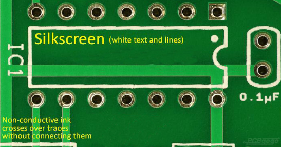
- Visual inspection under magnification
- Solderability spot testing
- Surface finish thickness verification
- Maintain records for traceability
3. Design Considerations
- Pad geometry optimization for good solder flow
- Thermal relief design for even heating
- Surface finish selection based on application requirements
- Solder mask design to prevent solder wicking
Troubleshooting Flowchart for Solder Wetting Issues
When confronted with solderability problems, follow this systematic approach:
- Visual Inspection:
- Check for obvious contamination or oxidation
- Examine surface finish integrity
- Process Verification:
- Confirm soldering temperature profiles
- Check flux application and activity
- Surface Testing:
- Perform simple water break test
- Conduct solder dip test if available
- Root Cause Analysis:
- Determine if issue is global or localized
- Check PCB storage conditions and age
- Corrective Action:
- Apply appropriate cleaning or surface treatment
- Adjust process parameters as needed
- Contact PCB supplier if issue appears manufacturing-related
Conclusion
PCB solderability issues present significant challenges in electronics manufacturing, but with proper understanding and methodology, they can be effectively addressed. The key to success lies in:
- Prevention: Proper storage, handling, and supplier selection
- Preparation: Appropriate surface cleaning and treatment
- Process Control: Optimized soldering parameters and atmosphere
- Problem-Solving: Systematic troubleshooting approach
By implementing the solutions outlined in this guide, manufacturers can significantly reduce solderability-related defects, improve production yields, and enhance product reliability. Regular solderability testing and process monitoring should be integral parts of any quality electronics manufacturing operation to catch potential issues before they affect production.
Remember that solderability problems often have multiple contributing factors. A comprehensive approach that addresses materials, processes, and environmental factors will yield the best results in achieving consistent, reliable solder joints on PCBs.


