How to improve PCB graphic electroplating film
I. Introduction:
With the rapid development of the PCB industry, PCB is gradually moving towards high-precision fine lines, small apertures, and high aspect ratios (6:1-10:1). The hole copper requirement is 20-25Um, and the DF line spacing is ≤4mil. Generally, PCB production companies have electroplating film problems. Film will cause direct short circuits, affecting the first yield of the PCB board through AOI inspection. Severe film or too many points cannot be repaired and directly lead to scrap.
II. Graphic electroplating film problem diagram:
PCB board film principle analysis
① The copper thickness of the graphic electroplating circuit is greater than the dry film thickness, which will cause film. (The dry film thickness used by general PCB factories is 1.4mil)
② The copper thickness and tin thickness of the graphic electroplating circuit exceed the dry film thickness, which may cause film.
- Analysis of the causes of PCB film clamping
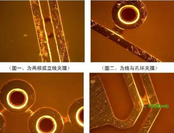
- Pictures and photos of easy-to-clip boards
Figure 3 and Figure 4 show that the circuits are densely packed from the photos of the actual boards. The length-width ratio of the engineering design layout is quite different, which is not conducive to current distribution. The minimum line gap of D/F is 2.8mil (0.070mm), the minimum hole is 0.25mm, the board thickness is 2.0mm, the aspect ratio is 8:1, and the hole copper requirement is >20Um or more. It is a difficult board for process.
2.Analysis of the causes of film clamping
① The current density of graphic electroplating is large, and the copper plating is too thick.
② The two ends of the flying bar are not clamped with edge strips, and the high current area is thickly plated.
③ The fault of the fire bull is larger than the set current of the actual production board.
④ The C/S surface and the S/S surface are hung upside down.
⑤ The spacing is too small. The board is clamped with a spacing of 2.5-3.5mil.
⑥ The current distribution is uneven, and the anode has not been cleaned in the copper plating tank for a long time.
⑦ Wrong current (wrong model or wrong board area)
⑧ Equipment failure. The PCB board of the broken machine is in the copper cylinder protection current for too long.
⑨ The layout design of the project is unreasonable, and the effective electroplating area of the project provided is incorrect.
⑩ The line gap of the PCB board is too small, and the circuit graphics of the high-difficulty board are easy to be sandwiched.
3.Effective improvement plan for sandwich
- Reduce the current density of the graphics and appropriately extend the copper plating time.
- Appropriately thicken the copper plating thickness of the board, appropriately reduce the copper plating density of the graphics, and relatively reduce the copper plating thickness of the graphics.
- The bottom copper thickness of the pressure plate is changed from 0.5OZ to 1/3OZ bottom copper pressure plate. Thicken the copper plating thickness of the board by about 10Um, reduce the current density of the graphics, and reduce the copper plating thickness of the graphics.
- Purchase 1.8-2.0mil dry film for trial production for boards with a spacing of 4mil.
- Other solutions such as changing the layout design, modifying compensation, moving the line gap, cutting the hole ring and PAD can also relatively reduce the occurrence of film.
4.Electroplating production control method for boards with small line gaps and easy to be filmed
- FA: First try a Feiba board with edge strips at both ends of the Feiba. After the copper thickness, line width/line spacing, and impedance are qualified, the Feiba board is etched and inspected by AOI. If film is found, adjust the current immediately and retry FA.
- Film stripping: For boards with a D/F line gap of 4mil, the etching and film stripping speed is appropriately slowed down.
- FA personnel skills: Pay attention to the current density evaluation when the current indication is given for boards that are easy to be filmed. Generally, for boards with a minimum line gap of 3.5mil (0.088mm), the electroplating copper current density is controlled at Q12ASF, which is not easy to produce film. Except for the circuit graphics with particularly high difficulty boards as shown below:
The minimum line gap of D/F of this graphic board is 2.5 mil (0.063mm). Under the condition of good uniformity of the gantry electroplating line of general manufacturers, it is difficult to escape the fate of being sandwiched. It is recommended that the graphics and electrical use Q10ASF current density test FA.
The minimum line gap of D/F of this graphic board is 2.5 mil (0.063mm). There are many independent lines and they are unevenly distributed. Under the condition of good uniformity of the electroplating line of general manufacturers, it is difficult to escape the fate of being sandwiched. The current density of graphic electroplating copper plating is 14.5ASF*65 minutes to produce sandwiched film. It is recommended that the graphics and electrical use Q11ASF current density test FA.
5 Personal experience and summary
Based on my many years of experience in PCB process, basically every PCB factory that makes boards with small line width and line gap will have more or less sandwich problems. The difference is that the proportion of bad sandwich is different in each factory. Some companies have few sandwich problems, and some companies have more sandwich problems. The following factors are analyzed:
- The PCB board structure type of each company is different, and the difficulty of PCB manufacturing process is different.
- The management mode and process methods of each company are different.
- From my years of accumulated experience, for boards with small line gaps, we must first pay attention to using only small current density and appropriately extend the copper plating time. The current indication is evaluated based on experience to use the current density and copper plating time. Pay attention to the clamping method and operation method. For boards with a minimum line spacing of ≤4mil, the FA-Flying Board must be checked by AOI for film clamping problems. At the same time, it plays a role in quality control and prevention, so that the probability of film clamping during mass production will be very small.
I personally think that good PCB quality requires not only experience and skills, but also good methods. Another point depends on the execution strength of the production department personnel.
Graphic electroplating is different from whole board electroplating. The main difference is that the circuit patterns of various types of boards need to be electroplated. Some board circuit patterns are unevenly distributed. In addition to fine line width and line spacing, there are also sparse, several isolated lines, independent holes and various special circuit patterns. Therefore, the author prefers to use FA (current indication) skills to solve or prevent the problem of thick film. The improvement action is small and the effect is fast, and the preventive effect is obvious.


