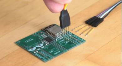
How to Improve PCB Pattern Plating Film Trapping Issues
Abstract
Pattern plating is a critical process in printed circuit board (PCB) manufacturing that creates conductive traces and pads. One persistent challenge in this process is film trapping, where plating solution becomes trapped between photoresist and copper surfaces, leading to various quality issues. This paper examines the root causes of pattern plating film trapping and provides comprehensive solutions to mitigate this problem. We explore process optimizations, material selections, equipment modifications, and quality control measures that can significantly reduce film trapping incidents in PCB production.
1. Introduction
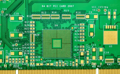
Printed circuit board manufacturing relies heavily on pattern plating processes to create the intricate copper traces that form electrical connections. During pattern plating, a photoresist is applied and patterned to expose areas where copper should be electroplated. However, a common issue known as “film trapping” occurs when plating solution becomes entrapped between the photoresist and copper surface. This trapped solution can lead to several problems:
- Uneven plating thickness
- Copper nodules and dendrite formation
- Resist adhesion failure
- Etching defects
- Reduced reliability of final product
Film trapping is particularly problematic in high-density interconnect (HDI) PCBs with fine features and tight spacing. As the industry moves toward smaller features and higher densities, addressing film trapping becomes increasingly important for maintaining yield and quality.
2. Root Causes of Film Trapping
Understanding the fundamental causes of film trapping is essential for developing effective solutions. The primary factors contributing to this issue include:
2.1 Photoresist Adhesion Issues
Poor adhesion between the photoresist and copper surface creates micro-gaps where plating solution can penetrate and become trapped. This can result from:
- Inadequate surface preparation before resist application
- Contamination on the copper surface
- Improper resist application parameters (thickness, soft bake)
- Resist formulation incompatibility with the copper surface
2.2 Process Parameter Variations
Deviations from optimal process parameters significantly affect film trapping:
- Inconsistent plating bath agitation
- Suboptimal current density distribution
- Improper racking or panel orientation
- Temperature fluctuations in plating baths
2.3 Equipment Design Limitations
Certain equipment configurations are more prone to causing film trapping:
- Insufficient solution flow in plating cells
- Poor anode-to-cathode geometry
- Inadequate rinsing station design
- Non-uniform spray patterns in processing equipment
2.4 Material Selection
The choice of materials impacts film trapping susceptibility:
- Resist type (dry film vs. liquid)
- Resist thickness and mechanical properties
- Plating chemistry formulation
- Copper foil characteristics
3. Strategies to Reduce Film Trapping
Based on these root causes, several strategies can be implemented to minimize film trapping in PCB pattern plating.
3.1 Surface Preparation Improvements
Enhancing the copper-resist interface is crucial for preventing solution penetration:
- Micro-etch optimization: Implement controlled micro-etching (typically 1-2 μm) to create optimal surface roughness for resist adhesion
- Cleaning processes: Use effective cleaning chemistries to remove oxides and contaminants
- Pre-treatment: Apply adhesion promoters where appropriate for challenging applications
3.2 Photoresist Process Optimization
Proper resist application and processing significantly reduces film trapping:
- Resist selection: Choose resists with appropriate mechanical properties (elastic modulus, elongation) for the application
- Application parameters: Optimize lamination temperature, pressure, and speed for dry films; or spin/spray parameters for liquid resists
- Post-application baking: Implement proper soft bake to remove solvents without over-curing
- Thickness control: Maintain consistent resist thickness appropriate for feature sizes
3.3 Plating Process Modifications
Adjusting plating parameters can help prevent solution entrapment:
- Agitation enhancement: Increase solution flow through eductors, spray bars, or ultrasonic agitation
- Current density optimization: Use simulation tools to optimize current distribution and minimize edge effects
- Pulse plating: Implement pulse or periodic reverse plating to allow solution refreshment in tight spaces
- Racking orientation: Position panels to promote solution drainage (typically 5-15° from vertical)
3.4 Equipment Upgrades
Modern equipment designs can significantly reduce film trapping:
- Spray systems: Install optimized spray nozzles with uniform coverage
- Anode design: Use conforming anodes or segmented anodes for better current distribution
- Rinsing stations: Implement high-pressure spray rinses between process steps
- Filtration: Maintain continuous filtration with appropriate micron ratings
3.5 Process Monitoring and Control
Implementing robust process control prevents conditions that lead to film trapping:
- Bath maintenance: Regular analysis and adjustment of plating bath chemistry
- Parameter monitoring: Continuous monitoring of temperature, flow rates, and current
- Quality checks: Regular cross-sectioning to verify plating uniformity
- Automation: Implement automated control systems for consistent processing
4. Advanced Solutions for Challenging Applications
For HDI and ultra-fine feature PCBs, additional measures may be necessary:
4.1 Modified Resist Technologies
- Sloped sidewall resists: Use resists that develop with tapered profiles to promote solution flow
- Elastomeric resists: Employ resists with enhanced flexibility to conform to surfaces
- Chemical amplification: Utilize chemically amplified resists for superior adhesion
4.2 Plating Chemistry Innovations
- Wetting agents: Incorporate surfactants that reduce surface tension
- Leveling additives: Use chemistry that promotes uniform deposition
- Low-entrapment formulations: Specialized plating chemistries designed for fine features
4.3 Alternative Process Approaches
- Direct metallization: Consider additive processes that eliminate pattern plating
- Semi-additive processes: Use modified SAP techniques for fine features
- Embedded components: Reduce surface features through component embedding
5. Quality Assurance and Troubleshooting
Implementing effective QA measures helps identify and correct film trapping issues:
5.1 Inspection Techniques
- Automated optical inspection (AOI): Detect plating irregularities early
- Cross-sectional analysis: Quantify plating uniformity and trapping
- Adhesion testing: Verify resist integrity after plating
5.2 Corrective Actions
When film trapping is detected:
- Identify the root cause through process mapping
- Implement short-term containment (rework procedures)
- Develop long-term corrective actions (process changes)
- Verify effectiveness through controlled testing
5.3 Continuous Improvement
- Maintain detailed process records for correlation analysis
- Conduct regular process audits
- Stay updated with new technologies and materials
6. Conclusion
Film trapping in PCB pattern plating is a multifaceted challenge that requires a systematic approach to resolve. By addressing surface preparation, resist processes, plating parameters, equipment design, and quality control, manufacturers can significantly reduce film trapping defects. As PCB technology advances toward finer features and higher densities, implementing these improvements becomes increasingly critical for maintaining product quality and manufacturing yield.
The most effective strategy combines multiple approaches tailored to the specific manufacturing environment. Process engineers should conduct thorough evaluations of their particular film trapping issues and systematically test potential solutions. With proper implementation, the incidence of film trapping can be reduced dramatically, leading to higher quality PCBs and improved production efficiency.
Future developments in resist technology, plating chemistry, and equipment design promise to further mitigate film trapping challenges, enabling the continued advancement of PCB technology. Manufacturers who proactively address these issues will be better positioned to meet the demanding requirements of next-generation electronic devices.