How to Judge PCB Quality at a Glance: A Comprehensive Guide
Printed Circuit Boards (PCBs) form the foundation of nearly all modern electronic devices, from smartphones to industrial equipment. The quality of a PCB directly impacts the performance, reliability, and longevity of the final product. For engineers, procurement specialists, and quality control professionals, the ability to quickly assess PCB quality is an invaluable skill. This 2000-word guide will provide you with systematic methods to visually evaluate PCB quality before any electrical testing.
I. Surface Inspection: The First Visual Assessment
1. Solder Mask Evaluation
The solder mask is the protective layer covering the copper traces, and its quality offers immediate visual clues about the PCB’s overall manufacturing standards:
- Uniformity: A high-quality solder mask should have consistent coloration across the entire board without streaks, blotches, or uneven areas. Variations in color often indicate inconsistent application or curing processes.
- Smoothness: Run your finger lightly across the surface (with proper ESD precautions). The surface should feel uniformly smooth without rough patches or noticeable texture variations.
- Edge Definition: Examine where the solder mask meets component pads. The edges should be sharp and well-defined, without bleeding onto pads or leaving excessive copper exposed. Poor edge definition suggests improper alignment during the mask application process.
- Gloss Level: While glossiness varies by solder mask type (matte, semi-matte, glossy), the chosen finish should be consistent across the entire board unless intentionally varied for specific areas.
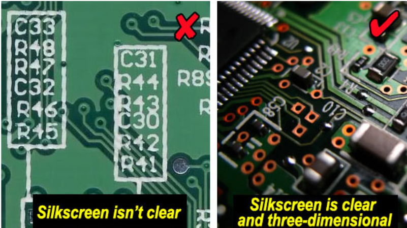
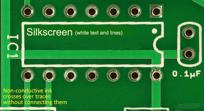
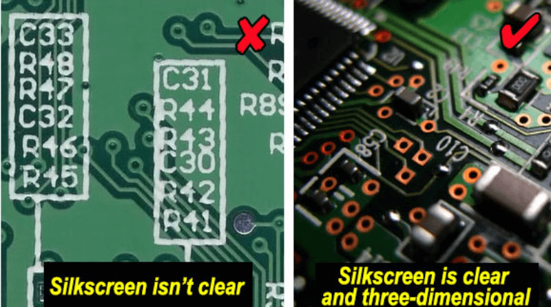
2. Silkscreen Quality Assessment
The silkscreen layer contains component labels, logos, and other markings that, while not electrically functional, reveal much about a manufacturer’s attention to detail:
- Legibility: All text and symbols should be crisp and easily readable under normal lighting conditions without magnification. Blurred or broken characters indicate poor printing processes.
- Alignment: Check that silkscreen elements are properly positioned relative to components and pads. Misaligned markings (especially polarity indicators) can lead to assembly errors.
- Completeness: Verify that all reference designators are present and match the assembly drawing. Missing labels suggest quality control oversights.
- Material Integrity: High-quality silkscreen ink shouldn’t chip or peel when lightly scratched with a fingernail (test in an inconspicuous area).
II. Physical Structure Examination
1. Board Thickness and Dimensional Accuracy
- Thickness Consistency: Measure board thickness at multiple points using calipers. Variations greater than ±10% of the specified thickness may indicate pressing or lamination issues.
- Outline Dimensions: Compare the actual board dimensions to the specified measurements. Pay special attention to edge connector areas and mounting holes where precision is critical.
- Layer Registration: Hold the board up to a bright light to check alignment of inner layers (for multilayer boards). Misregistration appears as uneven borders around the board edges.
2. Edge and Hole Quality
- Edge Smoothness: Board edges should be free of chips, cracks, or rough spots that could indicate poor depaneling methods. Examine edges under magnification for micro-fractures.
- Drill Quality: Inspect plated through-holes and vias:
- Holes should be cleanly drilled without residual debris or “haloing” around the edges
- No visible cracks or separation in the hole plating
- Consistent hole sizes without significant tapering
- Burr Inspection: Run a finger along hole edges (carefully) to detect burrs. Excessive burring suggests dull drill bits or improper drilling parameters.
III. Copper Features Inspection
1. Trace Quality Evaluation
- Width Consistency: Traces should maintain consistent width along their entire length. Narrowing or “necking” indicates potential etching problems.
- Edge Definition: Trace edges should be smooth without noticeable roughness or “mouse bites” (small indentations along the edges).
- Surface Condition: Copper should appear bright and clean without visible oxidation (darkening) or stains. Matte finishes may indicate poor surface preparation.
2. Pad Conditions
- Annular Ring Integrity: For through-hole pads, ensure there’s sufficient copper around the hole (typically at least 0.15mm for standard designs).
- Solderability: Pads should be free of oxidation, discoloration, or contamination that might affect solder adhesion. Fresh boards should have a slightly shiny appearance.
- Shape Consistency: All pads of the same type should have identical size and shape. Variations may indicate photolithography issues.
IV. Multilayer PCB Specific Checks
For multilayer boards, additional inspection criteria apply:
1. Interlayer Connection Quality
- Via Inspection: Examine several vias under magnification:
- Plating should appear uniform without voids or thin spots
- No resin protrusion (“nail heading”) into the via barrel
- Complete filling for filled vias without voids or depressions
- Blind/Buried Vias: These should show clean connections without signs of over-etching or misregistration.
2. Lamination Quality
- Delamination Signs: Look for any bubbles, puckering, or discoloration that might indicate poor bonding between layers.
- Resin Fill: Check that prepreg material completely fills all spaces between traces with no visible gaps or resin starvation.
V. Surface Finish Evaluation
The surface finish affects both solderability and long-term reliability:
1. HASL (Hot Air Solder Leveling)
- Even Coating: Solder should be uniformly distributed across pads without excessive buildup or skipping.
- Smoothness: The surface should be relatively flat without pronounced bumps or waves.
2. ENIG (Electroless Nickel Immersion Gold)
- Color Consistency: Should have uniform golden color without dark spots or discoloration.
- No “Black Pad”: Check for any dark areas in the nickel layer that might indicate “black pad” syndrome.
3. Immersion Silver/Tin
- Uniform Appearance: Should be shiny and free of oxidation or discoloration.
- No Whiskers: Examine under magnification for any metal whisker growth.
VI. Advanced Visual Inspection Techniques
For more thorough evaluation:
1. Magnified Inspection
Use 10X magnification to examine:
- Solder mask adhesion at trace edges
- Fine pitch component pads
- Microvia quality in HDI boards
2. Angled Lighting
View the board at various angles to detect:
- Subtle surface imperfections
- Solder mask thickness variations
- Plating inconsistencies
3. Comparative Analysis
Keep known-good sample boards for side-by-side comparison of:
- Color tones
- Surface textures
- Feature dimensions
VII. Common PCB Defects to Recognize
Train your eye to immediately spot these red flags:
- Measling/Webbing: White patches in the substrate indicating internal stress
- Delamination: Any visible separation between layers
- Plating Voids: Visible gaps in hole plating
- Over-etched Traces: Noticeably thinner than designed traces
- Solder Mask Skipping: Areas where copper is unintentionally exposed
- Contamination: Visible stains or residues
VIII. Correlation Between Visual Quality and Performance
While some visual defects are purely cosmetic, many correlate directly with reliability issues:
- Poor solder mask adhesion → Potential for dendritic growth and shorts
- Plating voids → Reduced current carrying capacity and potential open circuits
- Rough trace edges → Impedance variations in high-frequency circuits
- Contamination → Potential for electrochemical migration
IX. Limitations of Visual Inspection
While invaluable, visual examination has limitations:
- Cannot assess internal layer integrity in multilayer boards
- Doesn’t reveal electrical parameters like impedance or continuity
- Some materials defects require microscopic or SEM analysis
- Certain finishes (like OSP) may appear different but function perfectly
Therefore, visual inspection should complement rather than replace electrical testing and other quality control measures.
X. Developing Your PCB Evaluation Skills
To sharpen your PCB assessment abilities:
- Study IPC-A-600 standards for accept/reject criteria
- Examine both known-good and known-bad boards to train your eye
- Use consistent lighting conditions for evaluations
- Build a reference library of common defects
- Collaborate with experienced PCB manufacturers for insights
By systematically applying these visual inspection techniques, you’ll develop the ability to quickly assess PCB quality, identify potential issues early in the procurement process, and make informed decisions about board reliability. This skill becomes particularly valuable when qualifying new suppliers or evaluating prototype boards before committing to full production.
Remember that while visual inspection can identify many quality issues, it’s only one part of a comprehensive quality assurance program. Always combine visual checks with appropriate electrical testing and functional verification for complete quality assessment.