How to make flexible pcb in solidworks
Introduction To Designing Flexible PCBs In SolidWorks
Designing flexible printed circuit boards (PCBs) in SolidWorks is an intricate process that combines the principles of mechanical design with the nuances of electronic engineering. As technology advances, the demand for compact, lightweight, and flexible electronic devices has surged, making flexible PCBs increasingly popular. These PCBs are essential in applications where space constraints and mechanical flexibility are critical, such as in wearable technology, medical devices, and advanced consumer electronics. SolidWorks, a leading computer-aided design (CAD) software, offers robust tools to facilitate the design of these complex components, ensuring precision and efficiency.
To begin with, understanding the fundamental differences between rigid and flexible PCBs is crucial.
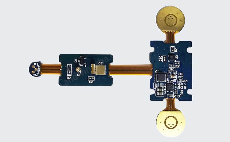
Unlike their rigid counterparts, flexible PCBs are made from materials like polyimide, which allow them to bend and twist without breaking. This flexibility introduces unique design challenges, such as managing stress points and ensuring reliable electrical connections. SolidWorks provides a comprehensive platform to address these challenges, offering features that allow designers to visualize and simulate the behavior of flexible circuits under various conditions.
The initial step in designing a flexible PCB in SolidWorks involves creating a detailed schematic of the circuit.
This schematic serves as a blueprint, outlining the electrical connections and components required for the PCB. SolidWorks’ integration with electronic design automation (EDA) tools streamlines this process, allowing for seamless import and export of schematic data. Once the schematic is complete, the next phase involves laying out the PCB.
This step is critical, as it determines the physical arrangement of components and traces on the board. SolidWorks’ PCB design tools offer a range of features, including auto-routing and design rule checks, to ensure that the layout is both efficient and manufacturable.
Transitioning from layout to 3D modeling, SolidWorks excels in providing a realistic representation of the flexible PCB.
The software’s 3D modeling capabilities allow designers to visualize the PCB in its final form, taking into account the bends and folds that characterize flexible circuits. This visualization is invaluable, as it enables designers to identify potential issues, such as component interference or excessive bending, before the manufacturing process begins. Moreover, SolidWorks’ simulation tools can predict the mechanical behavior of the PCB under various conditions, such as thermal expansion or mechanical stress, further enhancing the reliability of the design.
In addition to these technical aspects, SolidWorks also facilitates collaboration among design teams.
The software’s cloud-based platform allows multiple users to work on a project simultaneously, ensuring that all team members are aligned and informed throughout the design process. This collaborative environment is particularly beneficial in complex projects, where input from various disciplines is essential to achieve an optimal design.
In conclusion, designing flexible PCBs in SolidWorks is a multifaceted process that requires a deep understanding of both electronic and mechanical design principles. The software’s comprehensive suite of tools supports every stage of the design process, from schematic creation to 3D modeling and simulation. By leveraging these capabilities, designers can create flexible PCBs that meet the demanding requirements of modern electronic applications, ensuring both functionality and reliability. As technology continues to evolve, the ability to design flexible PCBs efficiently will remain a critical skill for engineers and designers alike.

Step-By-Step Guide To Creating Flexible PCB Layouts
Creating flexible PCB layouts in SolidWorks is a meticulous process that requires a blend of technical knowledge and precision. This step-by-step guide aims to provide a comprehensive understanding of how to navigate this process effectively. To begin with, it is essential to have a clear understanding of the design requirements and constraints. Flexible PCBs, unlike their rigid counterparts, offer the advantage of being able to bend and conform to different shapes, making them ideal for compact and dynamic applications. Therefore, the initial step involves defining the mechanical and electrical requirements of the PCB, which will guide the subsequent design process.
Once the requirements are established, the next step is to set up the SolidWorks environment for PCB design.
This involves installing the necessary add-ins or plugins that enable PCB design capabilities within SolidWorks. These tools are crucial as they provide the specific functionalities required for designing PCBs, such as layer management, trace routing, and component placement. With the environment set up, the designer can proceed to create a new project, ensuring that the project settings align with the design specifications, including the board dimensions and layer stack-up.
Transitioning to the design phase, the first task is to outline the board shape.
In SolidWorks, this is achieved by sketching the board outline on the top layer. It is important to accurately define the board’s dimensions and shape, as this will serve as the foundation for the entire design. Following this, the designer can begin placing components on the board. Component placement is a critical step that requires careful consideration of both electrical and mechanical constraints. Components should be placed in a manner that optimizes space while ensuring that electrical connections are feasible.
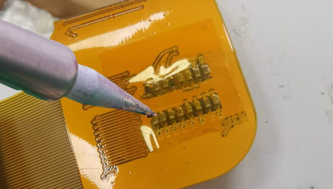
After placing the components, the next step involves routing the electrical traces.
This is where the flexibility of the PCB comes into play. The designer must ensure that the traces are routed in a way that accommodates the board’s bending and flexing without compromising electrical integrity. SolidWorks provides various tools to assist with trace routing, including auto-routing features and manual routing options. It is advisable to use a combination of both to achieve optimal results.
As the design progresses, it is crucial to continuously verify and validate the layout.
This involves running design rule checks (DRC) to ensure that the layout adheres to the specified electrical and mechanical constraints. Any errors or violations identified during this process should be addressed promptly to avoid issues during manufacturing.
Finally, once the design is complete and verified, the last step is to generate the necessary files for manufacturing.
SolidWorks allows for the export of Gerber files, which are the standard format used by PCB manufacturers. These files contain all the information required to fabricate the PCB, including the board layout, drill data, and component placements.
In conclusion, designing flexible PCBs in SolidWorks is a detailed process that requires careful planning and execution. By following this step-by-step guide, designers can effectively create flexible PCB layouts that meet their specific requirements. The key to success lies in understanding the unique characteristics of flexible PCBs and leveraging the tools available in SolidWorks to address these challenges.
Tips And Tricks For Optimizing Flexible PCB Designs In SolidWorks
Designing flexible PCBs in SolidWorks requires a nuanced understanding of both the software’s capabilities and the unique characteristics of flexible circuits. To optimize your flexible PCB designs, it is essential to leverage SolidWorks’ features effectively while considering the specific requirements of flexible electronics.
One of the first steps in this process is to ensure that you have a clear understanding of the mechanical and electrical constraints of your design. This involves defining the bend areas, which are critical in flexible PCBs, as they must withstand repeated flexing without compromising the circuit’s integrity.
To begin with, it is crucial to utilize SolidWorks’ advanced modeling tools to accurately represent the flexible PCB’s geometry.
This includes using the sheet metal feature, which, although traditionally used for metal parts, can be adapted to model the bending and folding characteristics of flexible PCBs. By setting appropriate bend parameters, you can simulate how the PCB will behave in real-world applications. Additionally, employing the flattening feature allows you to visualize the PCB in its flat state, which is essential for layout and component placement.
Transitioning from mechanical design to electrical considerations, it is important to integrate SolidWorks PCB, a tool that bridges the gap between electrical and mechanical design.
This integration facilitates seamless collaboration between ECAD and MCAD, ensuring that electrical components are accurately placed and that their connections are maintained throughout the design process. By synchronizing the electrical and mechanical aspects, you can prevent potential design conflicts and ensure that the flexible PCB meets all functional requirements.
Moreover, when designing flexible PCBs, it is vital to pay attention to the material properties and thicknesses.
SolidWorks allows you to define custom materials, which can be used to simulate the behavior of flexible substrates such as polyimide. By accurately modeling these materials, you can predict how the PCB will perform under various environmental conditions, such as temperature fluctuations and mechanical stress. This predictive capability is invaluable in optimizing the design for durability and reliability.
Another key consideration is the routing of traces on the flexible PCB.
In SolidWorks, you can use the routing tools to define the path of electrical traces, ensuring that they are placed in a manner that minimizes stress during bending. It is advisable to avoid sharp angles and to use curved traces, which distribute stress more evenly and reduce the risk of trace breakage. Additionally, maintaining consistent trace widths and spacing is crucial for signal integrity and overall performance.
Furthermore, SolidWorks provides simulation tools that can be used to analyze the mechanical behavior of the flexible PCB under various conditions.
By conducting finite element analysis (FEA), you can identify potential failure points and make necessary adjustments to the design. This proactive approach helps in optimizing the design for both performance and manufacturability.
In conclusion, optimizing flexible PCB designs in SolidWorks involves a comprehensive approach that integrates mechanical modeling, electrical design, material considerations, and simulation analysis. By leveraging the software’s capabilities and adhering to best practices, you can create flexible PCBs that are both functional and reliable. Through careful planning and execution, SolidWorks enables designers to push the boundaries of what is possible with flexible electronics, paving the way for innovative applications in various industries.

Common Challenges And Solutions In Flexible PCB Design Using SolidWorks
Designing flexible PCBs in SolidWorks presents a unique set of challenges that require careful consideration and innovative solutions. As the demand for compact and versatile electronic devices grows, the need for flexible PCBs has become increasingly prevalent.
These circuits offer the advantage of bending and folding to fit into tight spaces, making them ideal for modern electronic applications. However, the design process is not without its hurdles.
Understanding these challenges and their solutions is crucial for engineers and designers aiming to create efficient and reliable flexible PCBs using SolidWorks.
One of the primary challenges in designing flexible PCBs is managing the mechanical properties of the materials involved.
Unlike rigid PCBs, flexible circuits must withstand repeated bending and flexing without compromising their functionality. This requires a thorough understanding of the material properties, such as tensile strength and flexibility.
In SolidWorks, designers can utilize simulation tools to model the mechanical behavior of the PCB under various conditions. By simulating the bending and flexing processes, designers can predict potential failure points and make necessary adjustments to the design, ensuring the PCB can endure the required mechanical stresses.
Another significant challenge is the layout of the circuit traces.
In flexible PCBs, the traces must be carefully routed to avoid stress concentration points that could lead to cracking or breaking. SolidWorks provides advanced routing tools that allow designers to optimize trace paths, minimizing sharp angles and ensuring even distribution of stress across the board. Additionally, incorporating curved traces instead of sharp corners can significantly enhance the durability of the PCB. By leveraging these tools, designers can create layouts that are both efficient and robust, reducing the risk of mechanical failure.
Thermal management is also a critical consideration in flexible PCB design.
The compact nature of these circuits often leads to increased heat generation, which can affect performance and reliability. SolidWorks offers thermal simulation capabilities that enable designers to analyze heat distribution across the PCB.
By identifying hotspots and areas of concern, designers can implement effective cooling strategies, such as adding thermal vias or heat sinks, to dissipate heat efficiently. This proactive approach to thermal management ensures that the flexible PCB operates within safe temperature limits, enhancing its longevity and performance.
Moreover, the integration of components on a flexible PCB poses its own set of challenges.
The limited space and the need for flexibility require careful selection and placement of components. SolidWorks’ 3D modeling capabilities allow designers to visualize the entire assembly, ensuring that components fit within the designated space without interfering with the board’s flexibility. This holistic view of the design helps in identifying potential conflicts and making necessary adjustments early in the design process, reducing the likelihood of costly revisions later.
In conclusion, while designing flexible PCBs in SolidWorks presents several challenges, the software offers a suite of tools and features that can effectively address these issues.
By leveraging simulation capabilities for mechanical and thermal analysis, optimizing trace layouts, and carefully integrating components, designers can overcome the inherent challenges of flexible PCB design. As technology continues to evolve, mastering these techniques will be essential for creating innovative and reliable electronic devices that meet the demands of modern applications. Through a combination of technical expertise and the powerful capabilities of SolidWorks, designers can successfully navigate the complexities of flexible PCB design, paving the way for the next generation of electronic innovations.