How to make multilayer pcb
Understanding The Basics Of Multilayer PCB Design
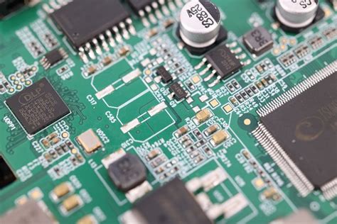
In the realm of modern electronics, multilayer printed circuit boards (PCBs) have become indispensable due to their ability to accommodate complex circuitry within a compact space.
Understanding the basics of multilayer PCB design is crucial for engineers and designers aiming to optimize the performance and reliability of electronic devices.
To begin with, a multilayer PCB consists of multiple layers of conductive material, typically copper, separated by insulating layers known as substrates. These layers are laminated together under high pressure and temperature to form a single, cohesive unit. The primary advantage of multilayer PCBs is their ability to support a higher density of components and interconnections compared to single-layer or double-layer boards.
The design process of a multilayer PCB starts with determining the number of layers required, which depends on the complexity of the circuit and the space constraints of the final product.
Typically, multilayer PCBs can range from four to as many as 20 or more layers. Once the number of layers is decided, the next step involves designing the stack-up, which is the arrangement of the conductive and insulating layers. A well-planned stack-up is essential for minimizing electromagnetic interference (EMI) and ensuring signal integrity. It is common practice to place power and ground planes on internal layers to provide a stable reference for signal layers and to reduce EMI.
Transitioning from the stack-up design, the focus shifts to routing the traces on each layer.
This involves creating pathways for electrical signals to travel between components. Effective routing is critical for maintaining signal integrity and minimizing crosstalk between adjacent traces. Designers often use computer-aided design (CAD) software to meticulously plan the routing, taking into account factors such as trace width, spacing, and via placement. Vias are small holes that allow connections between different layers, and their strategic placement is vital for efficient signal flow.
As the design progresses, attention must be paid to thermal management.
Multilayer PCBs can generate significant heat due to the high density of components and traces. Therefore, incorporating thermal vias, heat sinks, and appropriate materials can help dissipate heat effectively, preventing damage to the board and components. Additionally, selecting the right materials for the substrate and conductive layers is crucial for ensuring the board’s durability and performance under various environmental conditions.
Once the design is finalized, the manufacturing process begins.
This involves several steps, including the fabrication of individual layers, lamination, drilling of vias, and application of surface finishes. Each step must be executed with precision to ensure the final product meets the desired specifications. Quality control measures, such as electrical testing and inspection, are implemented to verify the board’s functionality and reliability.
In conclusion, understanding the basics of multilayer PCB design is a multifaceted process that requires careful consideration of various factors, from layer stack-up and trace routing to thermal management and material selection. By mastering these fundamentals, designers can create efficient and reliable multilayer PCBs that meet the demands of modern electronic applications. As technology continues to advance, the role of multilayer PCBs will undoubtedly expand, making it essential for professionals in the field to stay informed about the latest design techniques and manufacturing processes.
Essential Tools And Software For Multilayer PCB Creation
Creating a multilayer printed circuit board (PCB) is a complex process that requires a combination of specialized tools and software to ensure precision and functionality. The journey from concept to finished product involves several stages, each demanding specific resources to achieve the desired outcome. Understanding the essential tools and software for multilayer PCB creation is crucial for both novice and experienced designers.
To begin with, the design phase is critical, as it lays the foundation for the entire project. During this stage, computer-aided design (CAD) software is indispensable.
Programs such as Altium Designer, Eagle, and KiCad are popular choices among professionals. These tools offer a range of features that facilitate the design of intricate multilayer circuits, including schematic capture, layout design, and rule checking. The ability to simulate the circuit’s performance before physical production is a significant advantage, allowing designers to identify and rectify potential issues early in the process.
Transitioning from design to production, the next essential tool is a Gerber file generator.
Gerber files are the standard format for PCB manufacturing, containing all the necessary information about the board’s layers, including copper traces, solder masks, and silkscreens. Most CAD software can export designs into Gerber files, ensuring compatibility with manufacturing equipment. Additionally, a drill file, often in Excellon format, is required to specify the locations and sizes of holes on the PCB.
Once the design files are ready, the focus shifts to the physical creation of the PCB.
A multilayer PCB requires precise alignment and lamination of multiple layers, which is achieved using specialized equipment. A laminator is essential for bonding the layers together under heat and pressure, ensuring a durable and reliable board. Furthermore, an etching machine is necessary to remove excess copper from the board, leaving only the desired circuit paths. This process demands accuracy, as any deviation can lead to circuit failure.
In addition to these machines, inspection tools play a vital role in quality control.
These programs help designers assess how heat and electrical signals will behave within the board, which is particularly important for high-speed or high-power applications. By simulating these conditions, designers can make informed decisions about material selection and layer configuration, optimizing the board’s performance and reliability.
Moreover, software for thermal and signal integrity analysis is essential for multilayer PCB creation.
Optical inspection systems are used to verify the integrity of the PCB, checking for defects such as misaligned layers or incomplete etching. These systems often employ high-resolution cameras and automated software to detect issues that might be missed by the human eye. Ensuring the board meets the required specifications before assembly is crucial to avoid costly errors later in the process.
Finally, collaboration tools are invaluable for teams working on complex PCB projects.
Platforms that facilitate communication and file sharing, such as cloud-based project management software, ensure that all team members are aligned and informed throughout the design and production process. This collaborative approach helps streamline workflows and reduce the likelihood of errors.
In conclusion, the creation of multilayer PCBs is a multifaceted process that relies heavily on a combination of advanced tools and software. From design to production, each stage requires specific resources to ensure precision and quality. By leveraging these essential tools, designers can successfully navigate the complexities of multilayer PCB creation, ultimately delivering reliable and efficient electronic solutions.
Step-By-Step Guide To Manufacturing Multilayer PCBs
Manufacturing multilayer printed circuit boards (PCBs) is a complex process that requires precision and attention to detail. This intricate procedure begins with the design phase, where engineers use specialized software to create a detailed blueprint of the PCB. The design must account for the number of layers, the placement of components, and the routing of electrical connections. Once the design is finalized, it is converted into a format suitable for manufacturing, typically a Gerber file, which contains all the necessary information for each layer of the PCB.
Following the design phase, the next step is to prepare the materials.
Multilayer PCBs are composed of alternating layers of conductive copper and insulating material, usually a type of fiberglass known as FR-4. The process begins with the creation of the inner layers. Copper-clad laminates are cleaned and coated with a photosensitive film. This film is then exposed to ultraviolet light through a photomask, which transfers the circuit pattern onto the laminate. The exposed areas are developed, revealing the copper that will form the circuit traces. Unwanted copper is etched away using a chemical solution, leaving only the desired circuit pattern.
Once the inner layers are completed, they undergo an inspection process to ensure accuracy.
Any defects at this stage can lead to significant issues later in the manufacturing process. After inspection, the layers are laminated together under high temperature and pressure. This step involves stacking the inner layers with layers of prepreg, a resin-coated fiberglass material, and copper foil for the outer layers. The heat and pressure cause the prepreg to melt and bond the layers together, forming a solid multilayer board.
Drilling is the next critical step, where holes are created for component leads and vias, which are used to connect different layers of the PCB.
Precision drilling machines equipped with small, high-speed drill bits are used to ensure accuracy. After drilling, the holes are plated with copper to establish electrical connections between the layers. This is achieved through an electroplating process, where the board is submerged in a copper sulfate solution and an electric current is applied.
The outer layers of the PCB are then patterned using a similar process to the inner layers.
A photosensitive film is applied, exposed, developed, and etched to create the desired circuit pattern. Following this, a solder mask is applied to protect the copper traces and prevent solder bridges during component assembly. The solder mask is typically green, although other colors are available.
Finally, the PCB undergoes a surface finish process, which involves applying a coating to the exposed copper areas to protect them from oxidation and improve solderability.
Common finishes include HASL (Hot Air Solder Leveling), ENIG (Electroless Nickel Immersion Gold), and OSP (Organic Solderability Preservative). The finished PCB is then subjected to a series of electrical tests to verify its functionality and ensure there are no short circuits or open connections.
In conclusion, the manufacturing of multilayer PCBs is a meticulous process that requires careful planning and execution at each stage. From design to final testing, each step is crucial in producing a reliable and high-quality product. As technology continues to advance, the demand for more complex and compact PCBs will only increase, making the mastery of this process even more essential for manufacturers.
Common Challenges And Solutions In Multilayer PCB Fabrication
In the realm of electronics manufacturing, multilayer printed circuit boards (PCBs) have become indispensable due to their ability to support complex circuitry in a compact form. However, the fabrication of multilayer PCBs presents several challenges that manufacturers must navigate to ensure functionality and reliability. Understanding these challenges and their solutions is crucial for anyone involved in the design and production of multilayer PCBs.
One of the primary challenges in multilayer PCB fabrication is maintaining precise layer alignment.
As the number of layers increases, so does the complexity of aligning them accurately. Misalignment can lead to circuit failures and reduced performance. To address this, manufacturers employ advanced registration systems that use optical alignment techniques. These systems ensure that each layer is perfectly aligned with the others, minimizing the risk of misalignment and ensuring the integrity of the final product.
Another significant challenge is the management of thermal stress.
Multilayer PCBs often operate in environments where they are subjected to varying temperatures, which can cause expansion and contraction of the materials. This thermal cycling can lead to delamination, where layers separate, or cause micro-cracks in the vias and traces. To mitigate these issues, manufacturers use materials with low coefficients of thermal expansion and employ thermal management techniques such as the incorporation of thermal vias and heat sinks. These solutions help in dissipating heat effectively and maintaining the structural integrity of the PCB.
Signal integrity is also a critical concern in multilayer PCB fabrication.
As electronic devices become more sophisticated, the demand for high-speed data transmission increases. This necessitates careful consideration of signal integrity to prevent issues such as crosstalk, electromagnetic interference, and signal attenuation. To combat these problems, designers use techniques such as controlled impedance routing, differential pair routing, and the strategic placement of ground planes. These methods help in maintaining signal quality and ensuring that the PCB performs as intended.
Furthermore, the fabrication process itself poses challenges related to the drilling and plating of vias.
Vias are essential for establishing electrical connections between layers, but drilling them accurately in a multilayer stack can be difficult. Laser drilling and advanced mechanical drilling techniques are employed to achieve the precision required. Additionally, the plating process must ensure that vias are adequately filled and that there is a reliable electrical connection. This is often achieved through the use of advanced plating techniques such as direct metallization, which enhances the reliability of the vias.
Finally, the inspection and testing of multilayer PCBs are crucial to identify any defects that may have occurred during fabrication.
Traditional inspection methods may not be sufficient for multilayer boards due to their complexity. Therefore, manufacturers use advanced inspection technologies such as automated optical inspection (AOI) and X-ray inspection to detect defects that are not visible to the naked eye. These technologies allow for a thorough examination of the PCB, ensuring that any issues are identified and rectified before the board is deployed.
In conclusion, while the fabrication of multilayer PCBs presents several challenges, advancements in technology and manufacturing techniques have provided effective solutions. By addressing issues related to layer alignment, thermal stress, signal integrity, via drilling and plating, and inspection, manufacturers can produce reliable and high-performance multilayer PCBs that meet the demands of modern electronic devices.


