How to make rigid flex pcb
Understanding The Basics Of Rigid-Flex PCB Design
Rigid-flex PCBs, or printed circuit boards, are an innovative solution that combines the best features of both rigid and flexible circuits. These hybrid boards are increasingly popular in various industries, including aerospace, medical devices, and consumer electronics, due to their ability to provide enhanced reliability and design flexibility. Understanding the basics of rigid-flex PCB design is crucial for engineers and designers who wish to leverage these advantages in their projects.
To begin with, it is essential to comprehend the structure of a rigid-flex PCB.
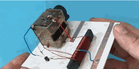
These boards consist of multiple layers of flexible circuit substrates attached to one or more rigid boards. The flexible layers are typically made from polyimide, a material known for its excellent thermal stability and flexibility, while the rigid sections are usually composed of traditional FR-4 material. This combination allows for the creation of a single, unified board that can be bent or folded to fit into complex or compact spaces, which is particularly beneficial in modern electronic devices where space is at a premium.
Transitioning to the design process, it is important to consider the unique challenges and requirements associated with rigid-flex PCBs.
One of the primary considerations is the need for precise layer stack-up planning. Designers must carefully determine the number of layers and their arrangement to ensure optimal performance and reliability. This involves balancing the electrical, mechanical, and thermal properties of the materials used, as well as considering the specific application and environmental conditions the PCB will face.
Moreover, the design of the flexible sections requires special attention.
These areas must be able to withstand repeated bending and flexing without compromising the integrity of the circuit. To achieve this, designers often incorporate features such as curved traces, staggered vias, and reinforced pads. Additionally, it is crucial to avoid sharp corners and stress points, which can lead to mechanical failure over time. By employing these strategies, designers can enhance the durability and longevity of the flexible sections.
Another critical aspect of rigid-flex PCB design is the integration of components.
Unlike traditional PCBs, where components are typically mounted on a single rigid surface, rigid-flex boards may require components to be distributed across both rigid and flexible sections. This necessitates careful planning of component placement and routing to ensure efficient signal transmission and minimize potential interference. Furthermore, designers must consider the impact of the board’s movement on component connections, ensuring that solder joints and other connections remain secure under dynamic conditions.
In addition to these technical considerations, it is also important to collaborate closely with manufacturers during the design process.
Rigid-flex PCBs require specialized fabrication techniques, and early communication with manufacturers can help identify potential issues and optimize the design for manufacturability. This collaboration can also aid in selecting the appropriate materials and processes to meet the specific requirements of the project.
In conclusion, understanding the basics of rigid-flex PCB design involves a comprehensive approach that considers the unique structural, mechanical, and electrical challenges these boards present. By carefully planning the layer stack-up, designing robust flexible sections, strategically placing components, and collaborating with manufacturers, designers can create reliable and efficient rigid-flex PCBs that meet the demands of modern electronic applications. As technology continues to evolve, the ability to effectively design and implement rigid-flex PCBs will become increasingly valuable, offering new possibilities for innovation and advancement in various fields.
Step-By-Step Guide To Manufacturing Rigid-Flex PCBs
Manufacturing rigid-flex PCBs involves a meticulous process that combines the benefits of both rigid and flexible circuit boards, offering enhanced reliability and design versatility. To begin with, the design phase is crucial, as it sets the foundation for the entire manufacturing process.
Engineers must carefully consider the layout, ensuring that the rigid and flexible sections are optimally integrated.
This involves using specialized software to create a detailed schematic that outlines the electrical pathways and component placements. Once the design is finalized, it is essential to conduct a thorough review to identify any potential issues that could arise during manufacturing.
Following the design phase, the next step is material selection.
Rigid-flex PCBs require a combination of materials that can withstand different environmental conditions while maintaining electrical integrity. Typically, the rigid sections are made from materials like FR-4, known for its durability and stability, while the flexible sections use polyimide, which offers excellent flexibility and thermal resistance. The choice of materials is critical, as it directly impacts the performance and longevity of the final product.
Once the materials are selected, the manufacturing process begins with the fabrication of the individual layers.
This involves etching the copper layers to create the desired circuit patterns. For the flexible sections, additional care is taken to ensure that the copper traces are designed to withstand bending and flexing without breaking. After etching, the layers are laminated together, with the flexible sections strategically placed between the rigid layers. This lamination process requires precise control of temperature and pressure to ensure a strong bond without damaging the delicate flexible circuits.
Subsequently, the drilled holes, known as vias, are created to establish electrical connections between the different layers.
This step is followed by plating the vias with copper to ensure reliable conductivity. The plating process must be carefully monitored to achieve the correct thickness, as this affects the board’s electrical performance and mechanical strength. After plating, the board undergoes a series of inspections to verify the integrity of the connections and the overall quality of the fabrication.
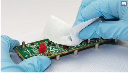
The next phase involves the application of a solder mask, which serves to protect the copper traces from oxidation and prevent solder bridges during component assembly.
The solder mask is typically applied using a photolithographic process, which ensures precise alignment with the underlying circuit patterns. Once the solder mask is applied, the board is ready for component assembly. This involves placing and soldering the electronic components onto the board, a process that requires precision and accuracy to ensure proper functionality.
Finally, the assembled rigid-flex PCB undergoes rigorous testing to verify its performance and reliability.
This includes electrical testing to check for continuity and shorts, as well as functional testing to ensure that the board operates as intended. Any defects identified during testing are addressed through rework or repair, ensuring that the final product meets the required specifications.
In conclusion, manufacturing rigid-flex PCBs is a complex process that demands careful attention to detail at every stage. From design and material selection to fabrication and testing, each step plays a vital role in producing a high-quality product that meets the demands of modern electronic applications. By following this step-by-step guide, manufacturers can achieve the precision and reliability necessary for successful rigid-flex PCB production.
Key Materials And Tools For Rigid-Flex PCB Fabrication
In the realm of modern electronics, the fabrication of rigid-flex printed circuit boards (PCBs) has become increasingly significant due to their versatility and efficiency. These PCBs combine the best attributes of rigid and flexible circuits, offering enhanced reliability and performance in complex electronic applications. To embark on the journey of creating a rigid-flex PCB, it is essential to understand the key materials and tools required for its fabrication. This knowledge not only ensures the successful production of the PCB but also optimizes its functionality and durability.
To begin with, the primary materials used in rigid-flex PCB fabrication include copper-clad laminates, polyimide films, and adhesive materials.
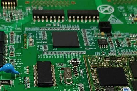
Copper-clad laminates serve as the foundational layer, providing the necessary conductive pathways for electronic signals. These laminates are typically composed of a thin copper foil bonded to a dielectric substrate, which can be either rigid or flexible depending on the design requirements. Polyimide films, on the other hand, are crucial for the flexible sections of the PCB. Known for their excellent thermal stability and mechanical properties, polyimide films allow the circuit to bend and flex without compromising its integrity. Adhesive materials are used to bond the different layers together, ensuring a cohesive structure that can withstand various environmental stresses.
In addition to these materials, several specialized tools are indispensable for the fabrication process.
One of the most critical tools is the PCB design software, which allows engineers to create detailed schematics and layouts of the circuit. This software is essential for planning the intricate pathways and connections that define the PCB’s functionality. Once the design is finalized, a photoplotter is used to transfer the circuit pattern onto a photomask, which is then employed in the photolithography process to etch the copper layers. This step is crucial for defining the precise conductive paths on the PCB.
Furthermore, drilling machines are required to create vias and holes that facilitate interlayer connections and component mounting.
These machines must be capable of high precision to ensure accurate alignment and connectivity. Following the drilling process, plating equipment is used to deposit a thin layer of metal, typically copper, onto the drilled holes and surface pads. This plating process enhances the electrical conductivity and mechanical strength of the connections.
As the fabrication progresses, lamination presses are employed to bond the various layers of the PCB together.
This step is particularly important in rigid-flex PCBs, as it involves the integration of both rigid and flexible sections into a single cohesive unit. The lamination process must be carefully controlled to prevent defects such as delamination or misalignment.
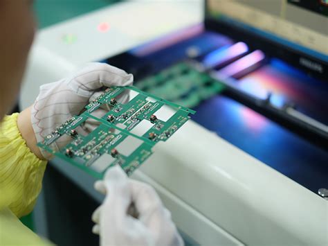
Finally, testing and inspection tools are essential to verify the functionality and quality of the finished PCB.
Automated optical inspection (AOI) systems and electrical testing equipment are commonly used to detect any defects or inconsistencies in the circuit. These tools ensure that the PCB meets the required specifications and performs reliably in its intended application.
In conclusion, the fabrication of rigid-flex PCBs necessitates a comprehensive understanding of the key materials and tools involved. By utilizing the appropriate materials such as copper-clad laminates, polyimide films, and adhesives, along with specialized tools like design software, photoplotters, and lamination presses, engineers can successfully create high-performance PCBs that meet the demands of modern electronic devices. This meticulous process not only enhances the functionality of the PCB but also ensures its durability and reliability in various applications.

Common Challenges And Solutions In Rigid-Flex PCB Production
In the production of rigid-flex printed circuit boards (PCBs), manufacturers often encounter a variety of challenges that can impact both the efficiency of the production process and the quality of the final product. Understanding these common challenges and their solutions is crucial for ensuring successful outcomes in rigid-flex PCB manufacturing.
One of the primary challenges in this domain is the complexity of the design process.
Rigid-flex PCBs combine the benefits of both rigid and flexible circuits, which necessitates a meticulous design approach to accommodate the different materials and their respective properties. To address this, designers must employ advanced design software that allows for precise modeling and simulation of the PCB layout. This software should facilitate the integration of both rigid and flexible sections, ensuring that the transition between these areas is seamless and that the overall design meets the required specifications.
Another significant challenge is the selection of appropriate materials.
The materials used in rigid-flex PCBs must withstand various environmental conditions, such as temperature fluctuations and mechanical stress, while maintaining electrical performance. To overcome this, manufacturers should carefully select materials that offer the necessary flexibility and durability. Polyimide is often used for the flexible layers due to its excellent thermal stability and mechanical properties, while FR-4 is commonly used for the rigid sections. By choosing the right combination of materials, manufacturers can enhance the reliability and longevity of the PCBs.
The manufacturing process itself presents additional challenges, particularly in terms of layer alignment and bonding.
Misalignment of layers can lead to electrical failures and reduced performance. To mitigate this risk, manufacturers should implement precise alignment techniques and utilize advanced equipment that ensures accurate layer registration. Furthermore, the bonding process, which involves attaching the flexible layers to the rigid sections, requires careful control of temperature and pressure to prevent delamination and ensure a strong bond. Employing automated bonding systems can help achieve consistent results and reduce the likelihood of defects.
Testing and quality assurance are also critical components of rigid-flex PCB production.
Given the complexity of these boards, thorough testing is essential to identify any potential issues before the PCBs are deployed in their intended applications. Manufacturers should conduct a series of tests, including electrical testing, thermal cycling, and mechanical stress testing, to verify the performance and reliability of the PCBs. Implementing a robust quality assurance program can help detect defects early in the production process, allowing for timely corrective actions and minimizing the risk of product failures.
Finally, cost management is a challenge that cannot be overlooked.
The intricate design and manufacturing processes associated with rigid-flex PCBs can lead to higher production costs compared to traditional PCBs. To address this, manufacturers should focus on optimizing their production processes to improve efficiency and reduce waste. This may involve investing in advanced manufacturing technologies, streamlining workflows, and implementing lean manufacturing principles. By doing so, manufacturers can achieve cost-effective production while maintaining high-quality standards.
In conclusion, while the production of rigid-flex PCBs presents several challenges, understanding these issues and implementing effective solutions can lead to successful outcomes. By focusing on design precision, material selection, manufacturing accuracy, rigorous testing, and cost management, manufacturers can overcome these challenges and produce reliable, high-performance rigid-flex PCBs that meet the demands of modern electronic applications