How to optimize PCB via design? Core details that electronic engineers cannot ignore
As a key link in PCB design, via design is crucial to the manufacturing and performance of PCB. In this article, we will analyze PCB via design to help electronic engineers complete hardware research and development more efficiently.
How to design the size of vias?
In the PCB manufacturing process, the material is cut first, that is, the large-sized copper clad board is cut into a specific specification substrate that meets the production requirements using an automatic cutter.
Large material
Then, a CNC drilling machine is used to accurately drill holes at the predetermined position on the copper clad board. Since the drill bit is round, it is impossible to drill a square hole.
For example, if a round ping-pong ball is placed at a right-angle corner, there will be a certain distance between the arc of the sphere and the right angle, which is called the “R angle”.
Drill tip
Like Jiali Chuang, mechanical drilling is used to process PCBs, and its drill tip specifications are in units of 0.05mm.
After checking the process parameters on Jiali Chuang’s official website, the specifications of the round hole drill are 0.15mm-6.30mm. If it is a slot hole, the minimum drill specification is 0.65mm, which is suitable for processing metallized slot holes; the minimum slot hole drill is 1.0mm, which is suitable for processing non-metallized grooves.
Therefore, when designing PCB, vias cannot be designed to any size.
What are the precautions for small hole design?
How big a hole is called a small hole? From the perspective of PCB manufacturing, 0.3mm is the dividing point, and holes smaller than 0.3mm are called small holes.
The smaller the via, the more difficult it is to process, especially when the via size is close to the process limit.
This problem is called the “depth ratio” problem in the industry. The depth ratio is defined as the ratio of the board thickness to the via diameter. The larger the depth ratio, the higher the processing difficulty. In other words, the smaller the via, the more difficult it is to process
There are three difficulties:
First, it is difficult to electroplating. The reduction in the aperture will make it difficult for the copper layer to be deposited evenly during the electroplating process, and it is easy to have problems with no copper or bad holes. Simply put, the smaller the via, the lower the copper deposition rate.
If PCB is produced in Jiali Chuang, in order to ensure the quality of PCB, Jiali Chuang will test the copper plating of the hole wall through a four-wire low-resistance test. Compared with traditional test methods, the four-wire low-resistance test has higher detection accuracy, detects bad hole problems in time, and ensures the reliability and quality of the product.

Second, the processing efficiency is low.
The shorter the effective length of the small hole drill, the fewer pieces can be drilled in the same batch during processing. This directly affects the production efficiency.
To avoid drill bit breakage, when drilling small holes, the equipment needs to reduce the feed speed and increase the rotation speed. This will not only prolong the processing time, but also increase the wear rate of the drill.
Therefore, when designing PCB, try to design the via size to be greater than 0.3mm to ensure processing efficiency and reduce costs. Only when space is limited, consider using small holes.
The third is the problem of outer diameter size.
When designing vias or welding holes, the size requirements of the inner diameter and outer diameter need to be considered. These parameters directly affect the manufacturing process of PCB. Taking Jiali Chuang as an example, the minimum processing parameters of double-sided boards and multi-layer boards are 0.15mm inner diameter and 0.25mm outer diameter.
Jiali Chuang can now produce high-layer boards with 6-32 layers.
With self-developed ultra-high-layer technology, via-in-disk technology and other technologies, the PCB produced by Jiali Chuang has a maximum number of layers of 32, a minimum aperture of 0.15mm, a minimum line width and line spacing of 0.0762mm, and supports hundreds of laminated structures. Especially the via-in-disk process, all high-layer boards with more than 6 layers use resin plugging + electroplating capping process, so that the vias can be directly punched on the pads, and the surface of the finished pads is smoother and the wiring space is larger.
Schematic diagram of via-in-disk process
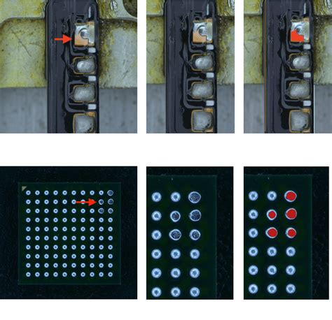
If the solder ring is too small, during the processing, the PCB may cause the center position of the drilled hole and the pad on the film to shift due to the deviation and alignment tolerance of the drilling equipment, resulting in a biased hole phenomenon.
This offset will reduce the effective area of the pad, increase the risk of manufacturing defects, and even cause electrical connection failure.
Therefore, it is crucial to reasonably design the size of the solder ring and consider the manufacturing tolerance to ensure the quality and reliability of the PCB.
What are the precautions for slot design?
Slots are another type of vias that cannot be ignored when designing PCBs. Especially in some special packages, slots are an indispensable design element.
When designing slots, there are two key points that need special attention:
First, “short slots” are the most difficult to process in PCB drilling. Slots with a slot length less than twice the slot width are called short slots. Since the slot length is less than twice the slot width, when the first hole is drilled and then the tail hole is drilled, the drill bit will be partially on the substrate and partially suspended. Under uneven force, the slot hole will be drilled crooked or short. Therefore, it is recommended that the optimal aspect ratio of the slot design is length/width ≧ 2.5.
Second, the long slot adopts the tin spraying process.
When designing slots, it is recommended to choose the tin spraying process, especially when the slot length exceeds 5mm, the ring width of the slot on both sides should be greater than 0.3mm (the limit is 0.2mm), or the immersion gold process should be used. If the slot ring width is less than 0.3mm, the tin spraying pressure is too large during the tin spraying process, which is prone to explosion problems. If the copper ring on one side of the hole meets the requirements, but there is no copper ring on the other side. This kind of slot with a single-sided copper ring is more susceptible to impact and causes explosions.
Tin spraying explosion (shown on the left and right)
When the slots are densely arranged, the longitude and latitude of the substrate may be damaged during the drilling process, which will cause explosion problems during tin spraying. For this special form of design, it is recommended to use the immersion gold process.
What is the difference between vias and component holes (Pads)?
In PCBs, the apertures are divided into vias (Via) and component holes (Pads), and they must not be mixed.
Vias generally play the role of conducting on both sides, and the processing process is generally to choose oil cover treatment.
Component holes (Pads) are usually designed as plug-in holes and used when plug-in soldering.
If vias (Via) and component holes (Pads) are mixed, one situation is that the via (Via) attribute is mistakenly used in the plug-in package as a component hole. When selecting via cover oil, the plug-in hole will be covered or blocked by ink, and the size cannot be effectively controlled.
Another situation is that the component hole (Pad) is mistakenly used as a via. When the software automatically closes the via window, it cannot be effectively identified, which will cause the via that needs to be covered with oil to be unable to be covered with oil.
Summary ● When designing PCB, vias cannot be designed to any size. ● From the perspective of PCB manufacturing, holes smaller than 0.3mm are called small holes. Small vias not only make PCBs difficult to electroplate, but also reduce processing efficiency. If the solder ring is too small, the hole may be biased. ● “Short slots” are difficult to process. It is recommended that the optimal aspect ratio of the slot hole be greater than or equal to 2.5. ● When designing slot holes, the ring width should be greater than 0.3mm (the limit is 0.2mm). It is recommended to choose tin spraying process or gold immersion process. ● Do not mix vias (Via) and component holes (Pad)