How to Place Inductors on a Switch-Mode Power Supply Printed Circuit Board
Introduction
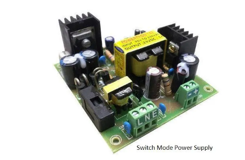
Switch-mode power supplies (SMPS) have become ubiquitous in modern electronics due to their high efficiency and compact size. One of the most critical components in any SMPS design is the inductor, which stores energy during the switching cycle and releases it to the output. Proper placement of inductors on the printed circuit board (PCB) is essential for achieving optimal performance, minimizing electromagnetic interference (EMI), and ensuring reliable operation. This article provides a comprehensive guide on inductor placement techniques for SMPS PCBs.
Understanding Inductor Characteristics in SMPS
Before discussing placement strategies, it’s important to understand how inductors function in switch-mode power supplies:
- Energy Storage: Inductors store energy in their magnetic field during the on-time of the switching cycle and release it during the off-time
- Current Filtering: They smooth out the pulsed current from the switching element
- Noise Generation: Inductors can be sources of both conducted and radiated EMI due to their magnetic fields
- Heat Dissipation: Power inductors often handle significant current and may require thermal considerations
Fundamental Placement Guidelines
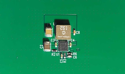
1. Proximity to Switching Elements
Place the inductor as close as possible to the switching element (MOSFET or power IC):
- Minimizes high-frequency current loop area
- Reduces parasitic inductance in the switching path
- Typical distance: 5-10mm for most designs
2. Orientation Considerations
Proper orientation of multiple inductors is crucial:
- Place adjacent inductors at 90° to each other to minimize mutual coupling
- Avoid parallel alignment of similar inductors to prevent unwanted transformer effects
- Consider the direction of magnetic flux when positioning near sensitive components
3. Layer Stackup and Return Paths
Optimize your PCB layer stackup for inductor placement:
- Place inductors on layers adjacent to solid ground planes
- Ensure uninterrupted return paths beneath the inductor
- Avoid splitting ground planes beneath inductors
4. Thermal Management
Address thermal considerations in placement:
- Provide adequate copper area for heat dissipation
- Consider thermal relief connections for wave soldering
- Maintain proper clearance from heat-sensitive components
Advanced Placement Techniques
1. Loop Area Minimization
The primary goal in SMPS layout is to minimize high-current loop areas:
- Identify the critical high di/dt paths (switch-inductor-output capacitor)
- Arrange components to create the smallest possible loop
- Use the “first floor” technique – imagine components placed directly above each other through layers
2. Shielding Strategies
For designs sensitive to EMI:
- Consider using shielded inductors in noise-sensitive applications
- Implement partial PCB shields around unshielded inductors
- Use ground stitching vias around the inductor perimeter
3. Multi-Inductor Designs
For power supplies with multiple inductors (e.g., multi-phase converters):
- Maintain equal trace lengths to each inductor when possible
- Follow symmetry in placement for balanced current sharing
- Consider interleaving inductor positions for better thermal distribution
4. High-Frequency Considerations
For high-frequency SMPS designs (≥1MHz):
- Account for parasitic capacitance in placement
- Minimize via count in high-current paths
- Consider the effects of proximity to board edges
Common Placement Mistakes to Avoid
- Excessive Distance from Switching Node: Increases loop area and EMI
- Improper Grounding: Creating ground loops or split planes beneath the inductor
- Inadequate Clearance: Not providing enough space for magnetic flux
- Poor Thermal Design: Overlooking heat dissipation requirements
- Ignoring Mechanical Stress: Not accounting for vibration or board flexure
Practical Implementation Steps
Follow this step-by-step approach for optimal inductor placement:
- Identify Critical Paths: Map out the high-current loops in your schematic
- Create Placement Zones: Define areas for power components, control circuitry, etc.
- Position Switching Elements: Place MOSFETs or power ICs first
- Place Inductors: Adjacent to switches with proper orientation
- Arrange Supporting Components: Position input/output capacitors next
- Verify Loop Areas: Visually inspect high-current paths
- Check Thermal Distribution: Ensure adequate heat spreading
- Review for EMI Concerns: Consider magnetic field interactions
Simulation and Verification
Before finalizing your layout:
- Use field solvers to analyze magnetic flux distribution
- Perform thermal simulations if dealing with high currents
- Verify current density in traces using DC analysis tools
- Check for voltage drops in high-current paths
Case Studies
Case Study 1: Buck Converter Layout
In a typical buck converter:
- The critical loop is from the input capacitor through the high-side switch, inductor, to the output capacitor
- Place the inductor between the switch node and output capacitor
- Keep all three components (input cap, switch, inductor) on the same side of the board when possible
Case Study 2: Multi-Phase VRM Design
For voltage regulator modules with multiple phases:
- Arrange inductors in a symmetrical pattern
- Maintain equal trace lengths to each phase
- Consider thermal distribution across the board area
Manufacturing Considerations
Factor in these production aspects:
- Automated Assembly: Ensure pick-and-place machine accessibility
- Wave Soldering: Provide proper thermal relief for through-hole inductors
- Inspection: Allow adequate space for visual or AOI inspection
- Rework: Consider access for potential rework operations
Future Trends in Inductor Placement
Emerging technologies affecting inductor placement:
- Integrated Magnetics: Components combining inductors and transformers
- Embedded Inductors: Inductive elements within PCB layers
- 3D Packaging: Vertical stacking of power components
- Advanced Materials: Higher frequency core materials enabling smaller sizes
Conclusion
Proper inductor placement in switch-mode power supply PCBs is both an art and a science. By understanding the fundamental principles, avoiding common mistakes, and implementing advanced techniques, designers can create layouts that optimize performance, reliability, and manufacturability. Remember that each design presents unique challenges, and the best placement strategy often requires balancing multiple competing requirements. Through careful planning, simulation, and verification, you can achieve optimal inductor placement in your SMPS designs.


