How to prevent Contamination on pcbs
Ensuring chemical compatibility isn’t always as simple as avoiding adding fuel to the fire. When I was an undergraduate, I worked in a lab, specifically focusing on etching. The processing steps use a range of chemicals, sometimes incompatible. One day, my student colleague heard a strange noise while etching. A few minutes later, he closed the fume hood and was met with a small explosion of incompatible chemicals. Thankfully, he wasn’t injured; however, several weeks of work were ruined because he had to leave something on his wafer during processing.
While contamination doesn’t always have dramatic consequences like an explosion, it almost always has adverse and frustrating effects. On PCBs, contamination often more subtly impairs functionality, destroys insulation, and causes shorts—the end result is still a loss of your hard work. Understanding what contamination is and how it arises is the first step to avoiding it in future processing and designs.
The Impact of Contamination
Contamination may sound bad, but what does it mean for your PCB? It depends on the contaminant, but it generally degrades elements enough to impair functionality. Electrical issues are most common, with corrosion damaging insulation and conductors. This can lead to power loss, failures, and even shorts. While you can inspect the power delivery network for damage, it’s best to do everything possible to avoid contamination damage.
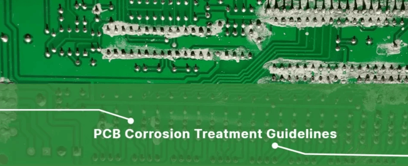
Electrochemical migration is one of the most concerning issues. When ions are left on the circuit board, often by etchants or other chemicals, the electrical potential can cause “reverse plating,” pulling metal away from where you want it and re-depositing new “traces”—traces that act like tiny, destructive PCB gremlins, causing trouble and strife. These small traces (called dendrites) create bridges, shorting the entire PCB. They also often burn and reform, making them difficult to track and diagnose.
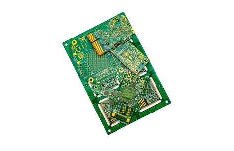
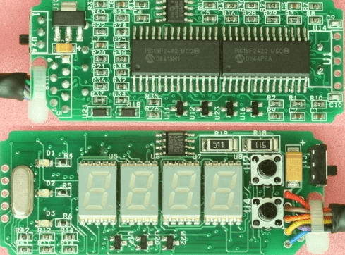
Contamination on PCBs
Contamination comes from any environmental source that should be removed, from skin oils to solvent residue. Depending on the type of contamination and where it occurs, a variety of problems can arise. The most common is degradation and accelerated deterioration of metallized surfaces, polymers, and masking. Areas around wirebond interconnects are particularly vulnerable. Other process steps that can contaminate the board include:
Solder paste handling: The solder paste applied to the board can also become contaminated. If purchased from a reputable supplier, the solder paste itself should be fine, but contaminants can enter the paste during the application and reflow processes. Stencil printers and PCB surface treatments are also potential sources for picking up and spreading solder contamination. Flux residue can also remain on the PCB and act as a contaminant. Any impurities or foreign matter are particularly problematic for solder because they can cause tin whiskers, which can create electrical shorts between solder joints or traces.
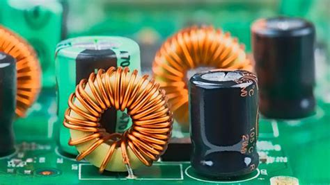
Etchant and Chemicals: If you examine the PCB manufacturing process, you’ll find a variety of acids and potentially harmful chemicals used during processing. Etching is an obvious source of acid, but flux, electrolyte solutions, and water-soluble solder all leave chemical residues on the board after application and use. After any chemical process, the board needs to be cleaned to ensure no residue remains that could contaminate the next manufacturing stage.
Some contaminants can burn the board, but it’s difficult to say how serious it is when the PCB is smoking.
Prevention
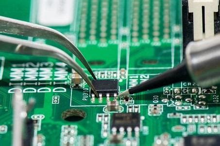
Preventing contamination is a best practice for both you and your PCB design. Unfortunately, humans are a source of contamination, with skin cells and hair deposited on the board during manufacturing, especially if it’s not done in a cleanroom. Human handling can also leave oils on the PCB, making it a particularly difficult source of cross-contamination. These oils are particularly difficult to remove. Taking precautions to ensure your skin or hair doesn’t contaminate circuit boards and handling your products in a clean environment are good first steps to avoiding these contaminants.
Ensuring your manufacturer also maintains a clean production environment with strong process controls is a second step in preventing contamination. Verify the quality of the materials used, especially solder mask and flux-containing solder. Some manufacturers will also test for chemical residues during processing. The most common method involves immersing a sample board in a solution and measuring the ionic changes in the solution as the chemical dissolves from the PCB. If you have issues with chemical residues, you can learn more about specific tolerances for contamination in standard IPC-TM-650, Method 2-3-25.
PCBs need to be cleaned between chemical applications, although hose cleaning isn’t always the right approach.
Contamination on PCBs can have disastrous consequences for your work, wasting valuable time and money. However, with proper maintenance and handling management, you can take preventative measures to ensure that PCB contamination minimizes the impact on your design’s manufacturing. However, it’s best to address the problem upfront by using excellent tools and processes, starting with the design software.