How to Properly Layout a 40A Power Supply: Copper, Vias, and Loops
1.Introduction
Current current demands have increased significantly, but the overall solution size continues to shrink. To accommodate, we can reduce the size of the buck converter, but it still must be able to handle the increasing power consumption in electronic systems. Optimizing the layout to improve the efficiency of the buck converter will reduce the amount of power required to power the system.
Many electronic systems require multiple buck converters to power different power rails. Some systems may require two or more converters to power a single rail with high current demands. The challenge of designing a smaller buck converter to meet this demand becomes a daunting task, but it is possible.
New technologies and processes are now in place that enable integrated circuit (IC) designers to design buck converters with a single output that can handle up to 40A. However, this capability introduces other issues. One is printed circuit board (PCB) layout. We can design the best buck converter and power stage given the space constraints, but all is lost if we fail to lay out the PCB correctly.
With 40A per output, PCB layout is critical for heat dissipation and efficiency. Without optimizing the board design, DC losses at 40A can increase significantly due to the higher resistance of the buried copper area. Therefore, in this post, I will explain the importance of copper area, via size and number, and current return path on multi-layer boards.
2.Copper Area
If the cross-sectional area (thickness x width), length, and resistivity of the copper are known, the resistance of a copper trace, plane, or copper pour can be calculated. With this data, the copper size can be determined to optimize the thermal, efficiency, and signal integrity performance of the PCB. Multi-layer boards with multiple buried copper layers connected to the top or bottom layers through vias also help to dissipate heat away from the IC. Figure #1 shows the efficiency difference between the switch node areas. The modified switch node area is larger than the original, reducing DC losses.
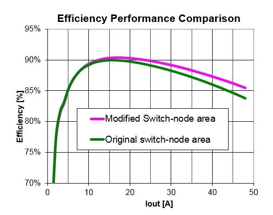
Figure 1: Modified switch node area showing size increase compared to the original switch node area
PCB traces, or copper conductors on a PCB, conduct signals on the surface of the PCB. What is left after etching is a narrow section of copper foil, and the current flowing through the copper lines generates a lot of heat. Properly calibrated PCB trace width and thickness help minimize heat buildup on the board. The wider the trace width, the lower the impedance to the current flow and the less heat buildup. PCB trace width is the horizontal dimension of the trace, while thickness is the vertical dimension of the trace.
PCB design always starts with a default trace width. However, such a default trace width is not always suitable for the desired PCB. This is because we need to consider the current carrying capacity of the trace to determine the trace width.
There are several factors to consider when determining the correct trace width:
- Copper layer thickness – Copper layer thickness is the actual trace thickness on the PCB, and the default copper thickness for high current PCBs is 1 ounce (35 microns) to 2 ounces (70 microns).
- Cross-sectional area of the conductor – To achieve higher power on the PCB, the trace must have a larger cross-sectional area, which is proportional to the trace width.
- Location of the trace – Bottom layer or top layer or inner layer.
3.via hole size and numbers
When vias connect two traces or planes together, they form a series resistance element. Typically, multiple vias in parallel reduce the effective resistance. Vias, like the area and thickness of flat copper, have a finite resistance. Therefore, we must optimize the number and size of vias to optimize the thermal performance and efficiency of the converter design.
Figures #2 and #3 represent two PCBs with the same setup and layout. The only difference is the number of vias on the IC thermal pad.
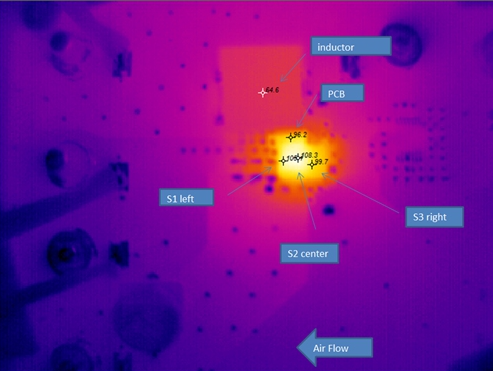
Figure #2: PCB with 11 vias under the thermal pad
*S2 (Site 2): Location of integrated FETs on the IC
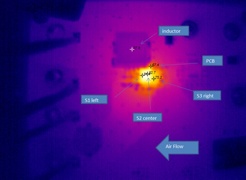
Figure #3: PCB with 35 vias under the thermal pad
4.Current Loops
We also need to optimize the current loop path between each alternate operating state of the high-side field effect transistor (FET) and the low-side FET in the buck converter. Our optimization should include the distance and current carrying capacity of the loop. Proper planning of the IC pinout design also becomes a factor in the PCB layout process. We should try to reduce the current loop area as much as possible.
As semiconductor technology and processes continue to advance, we are packing more silicon into the same package to enable higher current rated converter designs. For example, consider the new 40A SWIFT™ TPS543C20 synchronous buck converter with adaptive internal compensation and integrated NexFET™ MOSFETs. However, the basic question remains how to optimize the design so that we do not compromise thermal performance and efficiency. Hopefully, this article will help us properly create a true 40A power supply design with a smaller footprint.