How to Quickly Create a Switch Mode Power Supply PCB Layout Design
Introduction
Switch mode power supplies (SMPS) have become the backbone of modern electronic devices due to their high efficiency, compact size, and excellent power handling capabilities. However, designing an effective PCB layout for switch mode power supplies presents unique challenges that can make or break the performance of your power supply system. This comprehensive guide will walk you through the essential steps and best practices for quickly creating an optimized SMPS PCB layout while avoiding common pitfalls.
Understanding SMPS Fundamentals
Before diving into PCB layout, it’s crucial to understand the basic operation of switch mode power supplies:
SMPS Topologies
- Buck Converters: Step-down voltage regulators
- Boost Converters: Step-up voltage regulators
- Buck-Boost Converters: Provide both step-up and step-down capability
- Flyback Converters: Isolated power supplies common in AC/DC applications
- Forward Converters: Higher power isolated topologies
Key Components
- Power switches (MOSFETs)
- Inductors/transformers
- Capacitors (input, output, and bypass)
- Diodes or synchronous rectifiers
- Control IC with feedback network
Step 1: Schematic Design and Component Selection
A proper PCB layout begins with a well-designed schematic:
- Choose the Right Controller IC: Select an IC that matches your voltage, current, and topology requirements. Modern ICs often integrate power switches, reducing layout complexity.
- Calculate Component Values: Use manufacturer-provided design tools or formulas to determine:
- Inductor value (L)
- Input/output capacitor values
- Feedback network resistors
- Power switch ratings
- Consider Thermal Requirements: Estimate power dissipation to ensure components can handle thermal stresses.
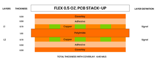
Step 2: PCB Stackup Design
Proper stackup is critical for SMPS designs:
- Layer Count: For simple designs, 2 layers may suffice. Complex designs may require 4 or more layers.
- Recommended Stackup:
- 4-layer board:
- Top Layer: Components and high-current traces
- Inner Layer 1: Ground plane
- Inner Layer 2: Power plane (if needed)
- Bottom Layer: Additional routing or second ground
- Copper Weight: Use 2 oz (70μm) copper for high current paths (>3A). Consider 3 oz or heavier for very high current designs.
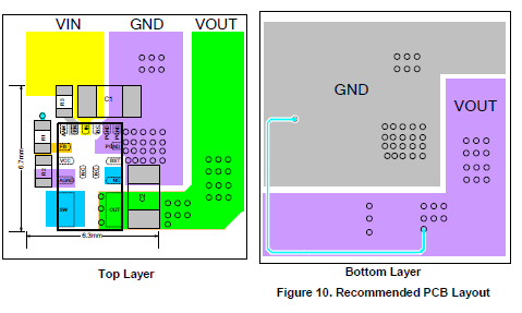
Step 3: Component Placement Strategy
Optimal component placement reduces noise and improves efficiency:
- Power Stage Placement:
- Place input capacitor close to the IC’s VIN pin
- Position the power switch (if discrete) near the controller
- Locate the inductor to minimize high-frequency current loops
- Place output capacitor near the inductor
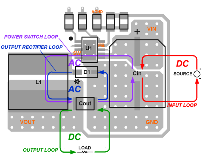
- Critical Paths:
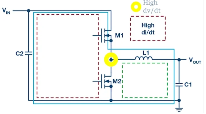
- Keep the switch node (connection between switch, diode, and inductor) as small as possible
- Minimize loop areas for high di/dt paths
- Thermal Considerations:
- Position heat-generating components with adequate spacing
- Consider thermal relief for components requiring heatsinking
Step 4: Routing Guidelines
Proper routing is essential for SMPS performance:
- High Current Paths:
- Use wide traces (minimum 20-50 mils per amp)
- Avoid 90° angles; use 45° angles or curved traces
- Utilize polygon pours for very high current paths
- Grounding Techniques:
- Implement a star ground for analog and power grounds
- Use separate ground planes for power and control sections if needed
- Connect grounds at a single point near the IC
- Sensitive Signals:
- Route feedback traces away from noisy areas
- Keep compensation networks close to the IC
- Avoid running sensitive traces parallel to high current paths
- Via Usage:
- Use multiple vias for high current connections (thermal and electrical reasons)
- Place vias close to component pads for better current flow
Step 5: Thermal Management
Effective thermal design prevents premature failure:
- Copper Area:
- Use large copper areas for heat dissipation
- Expose copper under components (if possible) for better heat transfer
- Thermal Relief:
- Add thermal vias under hot components
- Consider using copper pours on multiple layers connected with vias
- Heatsinking:
- Incorporate heatsinks for high-power components
- Ensure proper airflow in the final enclosure
Step 6: EMI Reduction Techniques
Switch mode supplies can generate significant electromagnetic interference:
- Layout Techniques:
- Minimize loop areas in high di/dt paths
- Keep high dv/dt nodes small (like switch nodes)
- Shield sensitive components with ground planes
- Filtering:
- Place input filters close to the power entry point
- Use proper bypass capacitor placement (high-frequency caps closest to IC)
- Shielding:
- Consider copper shields or cans for particularly noisy circuits
- Use guard rings around sensitive analog sections
Step 7: Design Verification
Before finalizing your layout:
- Design Rule Check (DRC):
- Verify all spacing and clearance requirements
- Check for unconnected nets
- Electrical Rule Check (ERC):
- Verify high current paths have sufficient width
- Check for potential short circuits
- 3D Visualization:
- Examine component placement in 3D to check for mechanical conflicts
- Verify heatsink clearances
Step 8: Prototyping and Testing
After PCB fabrication:
- Initial Power-Up:
- Use current-limited power supply
- Verify basic functionality before full power application
- Performance Testing:
- Measure efficiency at various loads
- Check for excessive ripple and noise
- Verify thermal performance under maximum load
- EMI Testing:
- Conduct radiated and conducted emissions tests
- Identify noise sources and consider layout improvements
Advanced Techniques for Optimized Layouts
For designers looking to push performance further:
- Current Mirroring: Duplicate critical paths on multiple layers to reduce resistance and improve thermal performance.
- Embedded Components: Consider embedding passive components in the PCB layers for space-constrained designs.
- Active Thermal Management: Incorporate temperature sensors and control loops to dynamically manage thermal performance.
Common Mistakes to Avoid
- Insufficient Copper for High Current Paths: Leads to excessive voltage drop and heating.
- Large Switch Node Loops: Creates EMI problems and reduces efficiency.
- Poor Grounding Schemes: Causes noise coupling and stability issues.
- Improper Component Placement: Leads to suboptimal performance despite good routing.
- Neglecting Thermal Considerations: Results in premature component failure.
Tools and Resources
- PCB Design Software:
- Altium Designer
- KiCad (open source)
- Cadence Allegro
- Mentor Graphics PADS
- Simulation Tools:
- LTspice (free from Analog Devices)
- SIMPLIS
- PSIM
- Manufacturer Resources:
- TI Power Designer
- Analog Devices LTPowerCAD
- Maxim Integrated EE-Sim
Conclusion
Creating an effective switch mode power supply PCB layout requires careful consideration of electrical, thermal, and electromagnetic factors. By following the systematic approach outlined in this guide—starting with proper schematic design, through thoughtful component placement and routing, to thorough verification—you can significantly reduce design iterations and achieve optimal performance on your first prototype.
Remember that SMPS layout is both an art and a science. While the guidelines presented here provide a solid foundation, each design presents unique challenges that may require creative solutions. With practice and attention to detail, you’ll be able to create high-performance switch mode power supply layouts quickly and efficiently.
As you gain experience, you’ll develop an intuition for identifying potential issues before they arise and optimizing layouts for specific applications. The key to success lies in understanding the fundamental principles, applying best practices consistently, and being willing to iterate when necessary.