How to Read a PCB: A Comprehensive Guide
Printed Circuit Boards (PCBs) are the fundamental building blocks of modern electronics. Understanding how to read and interpret PCBs is an essential skill for electronics engineers, technicians, hobbyists, and anyone working with electronic devices. This 2000-word guide will provide you with a structured approach to reading PCBs, covering all essential aspects from component identification to trace analysis.
Introduction to PCB Reading
Reading a PCB involves understanding its physical layout, electrical connections, and functional organization. Unlike schematic diagrams that show idealized circuit connections, PCBs represent the actual physical implementation of those circuits. This requires interpreting:
- Component placement and orientation
- Copper traces and their routing
- Layers and their interconnections
- Power and ground distribution
- Signal flow through the board
Developing PCB reading skills enables you to:
- Troubleshoot circuit issues more effectively
- Reverse-engineer existing designs
- Modify or repair electronic devices
- Understand design choices in commercial products
- Create better PCB layouts yourself
Section 1: PCB Fundamentals
1.1 Basic PCB Structure
Before reading a PCB, you must understand its basic construction:
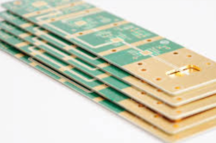
Substrate Material: Typically FR-4 (fiberglass epoxy), but can be ceramic, flexible material, or other specialized substrates.
Copper Layers: Thin copper foil laminated to the substrate, etched to form conductive paths. PCBs can be:
- Single-sided (one copper layer)
- Double-sided (two copper layers)
- Multi-layer (four or more copper layers)
Solder Mask: The colored coating (usually green) that insulates copper traces and prevents accidental shorts.
Silkscreen: White (typically) markings that show component designators, values, and other helpful information.
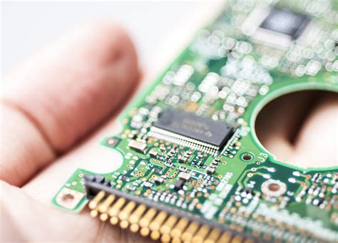
Vias: Plated-through holes that connect different layers of the PCB.
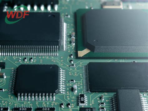
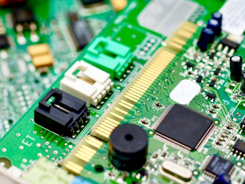
1.2 Common PCB Components
Recognizing components is the first step in reading a PCB:
Passive Components:
- Resistors (marked with R)
- Capacitors (marked with C)
- Inductors (marked with L)
- Diodes (marked with D)
Active Components:
- Integrated Circuits (ICs, marked with U)
- Transistors (marked with Q)
- Operational amplifiers (marked with U or IC)
Connectors:
- Headers (marked with J or P)
- Terminal blocks
- Board-to-board connectors
Electromechanical:
- Switches
- Relays
- Motors
Section 2: Systematic Approach to Reading PCBs
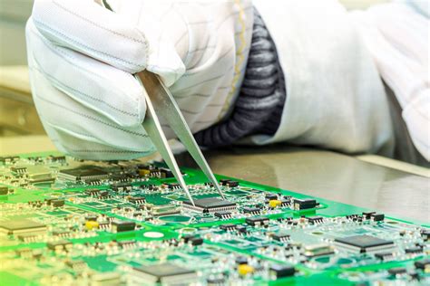
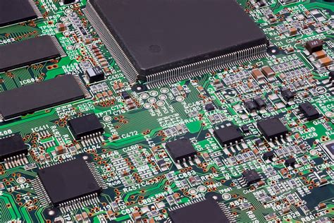
2.1 Visual Inspection
Begin with a thorough visual examination:
- Note the board’s physical characteristics:
- Dimensions and shape
- Mounting holes
- Connector locations
- Layer count (visible from the edge)
- Identify major components:
- Large ICs or processors
- Power components (voltage regulators, large capacitors)
- Connectors and interfaces
- Observe component groupings:
- Power supply section
- Digital processing area
- Analog signal chain
- RF section (if present)
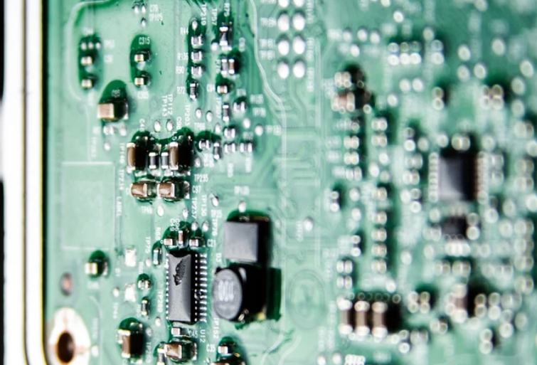
2.2 Understanding the Silkscreen
The silkscreen provides valuable information:
- Component designators:
- R1, R2, etc. for resistors
- C1, C2 for capacitors
- U1, U2 for ICs
- D1, D2 for diodes
- Component values:
- Resistor values (e.g., “10K” or “103” for 10kΩ)
- Capacitor values (e.g., “100μF 16V”)
- Polarity markings:
- Diodes and electrolytic capacitors
- IC orientation (notch or dot)
- Test points:
- Labeled points for measurement
- Often marked “TP1,” “TP2,” etc.
- Other markings:
- Version numbers
- Company logos
- Safety certifications
2.3 Trace Following Techniques
Following copper traces is fundamental to PCB reading:
- Start with power inputs:
- Locate where power enters the board
- Follow to voltage regulators
- Trace power distribution to components
- Identify ground connections:
- Look for ground planes (large copper areas)
- Note how components connect to ground
- Follow signal paths:
- Start at connectors or interfaces
- Trace through processing components
- Note signal conditioning elements
Tips for trace following:
- Use a bright light at a low angle to highlight traces
- For multi-layer boards, note via locations where traces change layers
- A magnifier or microscope helps with dense boards
- A continuity tester can verify connections
2.4 Multi-layer PCB Considerations
Reading multi-layer boards presents additional challenges:
- Layer identification:
- Outer layers (top and bottom) are visible
- Inner layers must be inferred or viewed through documentation
- Modern boards may have 4, 6, 8 or more layers
- Via types:
- Through-hole vias (connect all layers)
- Blind vias (connect outer to inner layers)
- Buried vias (connect only inner layers)
- Power and ground planes:
- Dedicated layers often serve as power distribution
- Ground planes provide return paths and shielding
Section 3: Advanced PCB Reading Techniques
3.1 Reverse Engineering Approaches
When documentation isn’t available, these methods help:
- Create a component list:
- Document all components with designators and values
- Note package types (SMD or through-hole)
- Draw connection diagrams:
- Sketch major component interconnections
- Highlight power and ground connections first
- Identify functional blocks:
- Group related components together
- Determine each block’s purpose (power supply, MCU, etc.)
3.2 Using Schematic Diagrams
When available, schematics greatly aid PCB reading:
- Cross-reference between schematic and PCB:
- Match component designators
- Verify physical layout matches schematic flow
- Understand schematic-to-PCB translation:
- Schematic shows logical connections
- PCB shows physical implementation
- Component placement affects routing
3.3 Signal Flow Analysis
Understanding signal paths is crucial:
- Input-to-output tracing:
- Start at input connectors
- Follow through processing stages
- End at output connectors
- Clock and data lines:
- Identify clock generators (crystals, oscillators)
- Trace clock distribution to ICs
- Note parallel or serial data buses
- Control signals:
- Reset lines
- Enable signals
- Interrupt lines
Section 4: Practical Applications
4.1 Troubleshooting with PCB Reading
PCB reading skills aid in fault finding:
- Power issues:
- Check power input to regulators
- Verify voltage at key points
- Look for damaged traces or components
- Signal problems:
- Verify signal continuity
- Check for proper terminations
- Look for unintended shorts
- Physical damage:
- Inspect for broken traces
- Check for cracked solder joints
- Look for burnt components
4.2 PCB Modification Techniques
Reading PCBs enables modifications:
- Adding components:
- Identify suitable connection points
- Consider impact on existing circuits
- Removing components:
- Understand the circuit implications
- Determine if jumpers are needed
- Rerouting traces:
- Carefully cut existing traces
- Add wire jumpers for new paths
Section 5: Tools for PCB Reading
5.1 Essential Tools
- Magnification:
- Magnifying glass
- Microscope (for dense boards)
- Measurement tools:
- Multimeter (continuity, voltage)
- Oscilloscope (signal analysis)
- Lighting:
- Bright, adjustable light source
- Side lighting for trace visibility
5.2 Advanced Tools
- PCB design software:
- Import board images for annotation
- Create reverse-engineered schematics
- X-ray inspection:
- For viewing inner layers
- Identifying hidden connections
- Thermal imaging:
- Locate hot spots
- Identify short circuits
Conclusion
Reading PCBs is both an art and a science that develops with practice. Start with simple single-layer boards and progressively tackle more complex designs. Remember these key points:
- Always begin with a systematic visual inspection
- Use the silkscreen information effectively
- Follow power and ground connections first
- Understand that physical layout differs from schematic organization
- Develop techniques for multi-layer boards
- Use appropriate tools to aid your analysis