How to reduce crosstalk in PCB boards
With the development of technology and people’s consumption needs, the trend of miniaturization of electronic devices is becoming more and more prominent, and printed circuit boards (PCBs) are getting smaller and smaller. This leads to unintentional coupling between signal traces in PCB boards, which is called crosstalk (as shown in Figure 1).
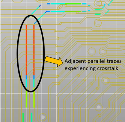
Figure 1. Parallel traces crosstalk
Here are some PCB wiring rules to reduce crosstalk.
Rule 1: Keep key signals away from I/O signals
It is necessary to pay special attention to the key wiring near the I/O connectors, because noise can easily leave or enter the circuit board through these I/O ports in the form of radiation or conduction. If the signal line directly connected to the I/O port is too close to the key signal line, a coupling effect will occur (see Figure 2).
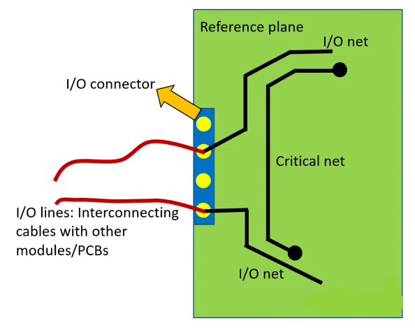
Figure 2. Key signal and I/O port routing diagram
Noise will enter through the I/O connection line and couple to the key signal (clock or sensitive signal) through the I/O connection line inside the PCB, as shown in Figure 3a. Similarly, the key signal (clock or high-speed signal) will couple the noise to the I/O signal routing inside the PCB and radiate outward through the I/O connection line, as shown in Figure 3b:
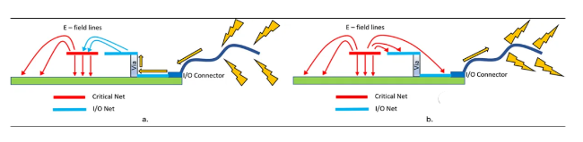
Figure 3. Key signals and I/O signals too close will cause potential EMC problems
Rule 2: High-speed signal routing is as short as possible
On high-speed PCBs (> 100MHz), high-frequency signals have a short wavelength and high radiation efficiency, so that the high-speed signal routing itself forms an antenna effect, especially when the routing is placed on the top or bottom layer. This unwanted radiation can couple to adjacent traces or even nearby interface connections. We recommend drawing high-speed signal traces on the middle layer of the PCB, as shown in Figure 4b. This helps control the electromagnetic field generated by high-speed signals and avoids unexpected coupling in the form of crosstalk or electromagnetic interference. If the high-speed trace is on the surface layer, the trace should be as short as possible. When the trace is smaller than the electrical minimum size (1/10 wavelength), the antenna effect will be greatly reduced. As shown in Figure 4:
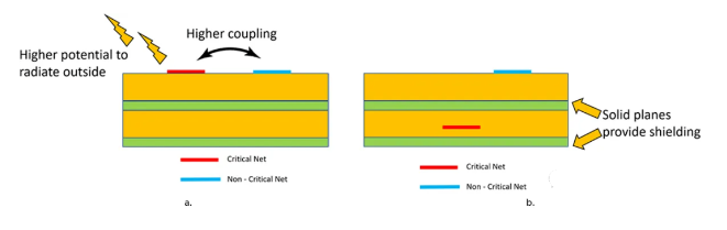
Figure 4. a. Signal on the surface layer b. Signal on the middle layer
Rule 3: Differential network matching
In theory, the signals transmitted by the differential pair are equal in size and opposite in polarity, so the EMI generated by the differential pair will cancel each other or be ignored. However, this is only effective when the differential pair traces are equal in length and as symmetrically close to each other as possible. Figure 5 shows differential pair traces in several different situations.

Figure 5. Comparison of the quality of differential routing
In order to compare the radiation of differential signal routing, the following circuit simulation is performed. Figure 6a and Figure 6b are two sets of symmetrical and asymmetrical routing, respectively. The high-frequency differential signal is input at the left end of the routing, and the load is terminated at the right end.
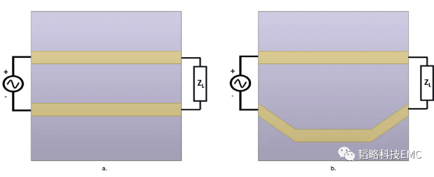
Figure 6. a. Symmetrical routing b. Asymmetric routing
We perform near-field analysis on the above two situations, and the noise simulation is shown in Figure 7:
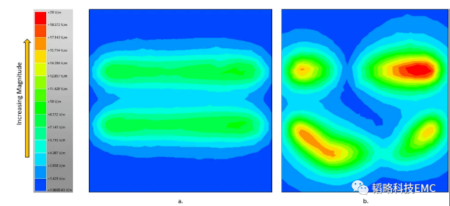
Figure 7. a Symmetrical differential routing simulation b Asymmetric differential routing simulation
At a distance of 1m, the radiation emission is compared and tested. In the frequency band of 30MHz-1GHz, the noise value of symmetrical routing is 8-10db lower than that of asymmetrical routing, as shown in Figure 8.
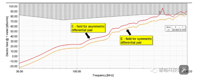
Figure 8. 1m distance radiation comparison data
In general, in the design of electronic equipment, the importance of early circuit design cannot be ignored. Good EMC design can ensure the normal operation of the equipment, avoid the impact of electromagnetic interference on other equipment, and improve the reliability of the product itself.