How to Reduce Ringing Through PCB Layout Techniques
Introduction
Ringing is a common signal integrity issue in high-speed digital circuits, characterized by unwanted oscillations that occur during signal transitions. These oscillations can lead to data corruption, increased electromagnetic interference (EMI), and reduced system reliability. Proper PCB layout techniques play a crucial role in minimizing ringing by controlling impedance, reducing parasitic effects, and optimizing signal return paths.
This article explores the causes of ringing and provides practical PCB layout strategies to mitigate it, ensuring robust high-speed circuit performance.
Understanding Ringing
Ringing occurs due to parasitic inductance and capacitance in a circuit, leading to resonance when a signal transitions (e.g., rising or falling edges). Key factors contributing to ringing include:
- Parasitic Inductance – Long traces, vias, and poorly designed return paths introduce inductance, which opposes rapid current changes.
- Parasitic Capacitance – Stray capacitance between traces, pads, and ground planes stores and releases energy, exacerbating oscillations.
- Impedance Mismatches – When the trace impedance does not match the source or load impedance, signal reflections occur, reinforcing ringing.
- Insufficient Damping – Lack of resistive damping allows oscillations to persist longer.
PCB Layout Techniques to Reduce Ringing
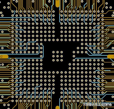
1. Optimize Trace Geometry for Controlled Impedance
- Use Proper Trace Width and Spacing – Follow impedance-controlled design rules to match the trace impedance (e.g., 50Ω for single-ended, 100Ω for differential pairs).
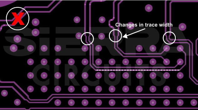
- Minimize Length Discontinuities – Avoid abrupt changes in trace width or layer transitions, which cause impedance mismatches.
- Use Microstrip or Stripline Configurations – Microstrip (surface traces over a ground plane) and stripline (traces sandwiched between ground planes) help maintain consistent impedance.
2. Reduce Parasitic Inductance and Capacitance
- Shorten High-Speed Signal Traces – Minimize trace lengths to reduce parasitic inductance.
- Avoid Sharp Corners – Use 45° bends or curved traces instead of 90° turns to minimize impedance discontinuities.
- Minimize Via Usage – Each via introduces inductance; if necessary, use multiple return vias near signal vias to reduce loop inductance.
3. Ensure a Solid Return Path
- Provide Uninterrupted Ground Planes – High-speed signals should have a continuous reference plane (preferably ground) beneath them.
- Avoid Splits or Gaps in Ground Planes – If a signal crosses a split in the reference plane, add a stitching capacitor nearby to maintain the return current path.
- Use Ground Pour and Stitching Vias – Fill unused board areas with ground copper and connect different ground layers with stitching vias to reduce loop inductance.
4. Terminate Signals Properly
- Series Termination (Source Termination) – Place a resistor (typically 10Ω–50Ω) near the driver to dampen reflections.
- Parallel Termination (Load Termination) – Use a resistor at the receiver end to match the trace impedance (e.g., 50Ω to ground for a 50Ω trace).
- AC Termination (RC Termination) – A capacitor in series with a termination resistor can help reduce power consumption while suppressing high-frequency ringing.
5. Manage Crosstalk and EMI
- Increase Spacing Between Critical Traces – Keep high-speed signals away from each other and from noisy lines (e.g., clocks, switching power traces).
- Use Guard Traces or Ground Shielding – Place grounded copper between sensitive traces to reduce crosstalk-induced ringing.
- Route Differential Pairs Tightly Coupled – Maintain consistent spacing between differential pairs to ensure common-mode noise rejection.
6. Select Appropriate PCB Materials
- Use Low-Loss Dielectrics – High-speed designs benefit from materials with stable dielectric constants (e.g., FR4 with tight tolerances or specialized RF laminates).
- Consider Thinner Dielectrics – Thinner substrates reduce loop inductance and provide better coupling to the ground plane.
7. Simulate and Validate the Design
- Perform Signal Integrity Simulations – Use tools like HyperLynx, ADS, or KiCad’s signal integrity analyzer to predict and mitigate ringing.
- TDR (Time Domain Reflectometry) Analysis – Helps identify impedance mismatches and reflections in the PCB layout.
- Prototype and Test – Measure signal quality with an oscilloscope to verify ringing suppression techniques.
Conclusion
Ringing in high-speed PCB designs can degrade signal integrity and lead to system failures. By implementing controlled impedance routing, minimizing parasitic effects, ensuring solid return paths, and using proper termination techniques, designers can significantly reduce ringing. Additionally, careful material selection, crosstalk management, and simulation-based validation further enhance signal quality.
Applying these PCB layout strategies ensures reliable high-speed signal transmission, reducing EMI and improving overall circuit performance. By understanding and mitigating the root causes of ringing, engineers can design more robust and efficient electronic systems.