How to reduce the noise of the circuit board
When we design the circuit board, the circuit principle is well designed, even excellent. However, various noises will appear during the debugging process, and the circuit board cannot achieve the expected purpose. Sometimes, even worse, the board has to be re-layed (although I have not encountered it, but I have encountered more than one or two other groups who have re-layed the board at work). So how can we reduce the noise of the circuit board? Let’s analyze it.
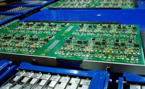
For a board with good performance, our EE can see its approximate distribution at a glance (the premise is to know what function this board has).
This is what we often call the principle of functional module separation. Functional module is a collection of circuits that combine some electronic components to complete a certain function. In actual design, we need to bring these electronic components closer and reduce the wiring length between electronic components to increase the role of circuit modules. In fact, this is not difficult to understand.
Our common development boards or mobile phones do this, especially mobile phones. If you disassemble the mobile phone, you will find that the modules are clearly separated, and each module is shielded by a Faraday cage.
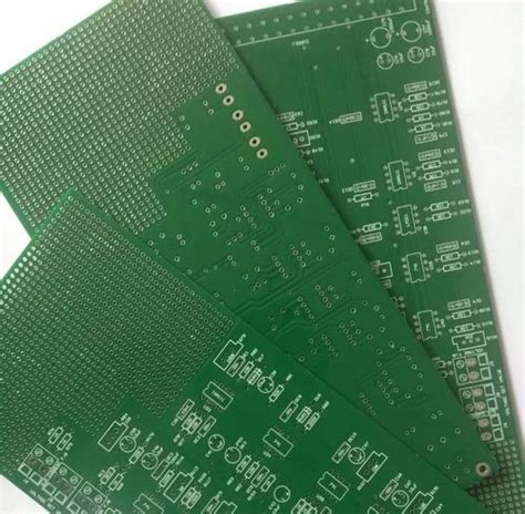
The above picture is a PCB of a development board. From the layout, it can be seen that the separation of each interface circuit is very clear, and the routing of SDRAM, DDR and SD card interface circuits will not cause mutual interference. By partitioning the system modules, it helps signal integrity, prevents high-frequency interference between system modules, and improves system stability.
Secondly, it should be noted that when there are analog and digital circuits on a PCB, the two need to be separated.
If you have to put a hat on it, there is a quiet zone. The so-called quiet zone is an area that physically isolates analog circuits from digital circuits or various functional modules. In this way, it can prevent other modules from interfering with the module. In the mobile phone circuit board mentioned above, the quiet zone is very obvious. Note that the quiet zone and the ground of the circuit board are not connected.
In actual circuit design, not every PCB board has enough space for us to make a quiet zone.
So, when space does not allow, how should we design it? I have summarized the following (I have not used them all, and some of them are even heard for the first time):
A. Use transformers or signal isolation components for design. The circuit separation composed of components such as CMOS or transistors is the meaning.
B. The signal passes through the filter circuit before entering the module. This method is a common method for preventing ESD. It is placed here because it can eliminate noise (ESD, high-frequency and high-voltage noise).
C. Use common-mode inductors to protect signals. A netizen once asked a question about this circuit protection method. If we don’t know the role of common-mode inductors, we will find that there are only two coils in the schematic diagram, which has no effect. In fact, it is not. It plays an important role in signal stability and noise interference elimination. This also reveals from another aspect that EE needs long-term training to grow.
A method similar to the quiet zone design of the circuit board is the trench protection technology.
This technology is to remove the copper foil of the quiet zone to form a bare circuit board material. The concept of the bridge is also derived from this: the power supply, ground and signal traces that connect each zone together are called bridges.
The trench protection technology has the ability to resist the impact of peak voltage and the tolerance of classic discharge protection, which plays a role in reducing circuit board noise to a certain extent. In the circuit board design, when the wiring unrelated to the isolation zone passes through the trench protection, RF loop current will be generated, which will affect the performance of the circuit board more. This needs to be noted.
Nowadays, many analog-to-digital or digital-to-analog components have connected the two grounds together inside the components, typically ADC and DAC devices. These devices need to be segmented and have a standard reference ground. If the digital signal current cannot effectively return to the source, it will cause noise and generate EMI. When drawing the schematic diagram, we found that there are AGND and DGND pins, which is a device with superior performance, which will reduce our design difficulty.
In general, the circuit is divided into modules and obvious quiet areas are set between the partitions to minimize the influence of power supply and ground on the signal and reduce the noise of the circuit board to the lowes