How to solve signal interference in the design of radio frequency printed circuit board (PCB)
With the development of electronic communication technology, wireless radio frequency circuit technology is more and more widely used. The performance index of radio frequency circuit directly affects the quality of the whole product. The anti-interference design of radio frequency printed circuit board (PCB) is of great significance to reduce the electromagnetic information radiation of the system. The density of radio frequency circuit board is getting higher and higher. The quality of PCB circuit board design has a great influence on the anti-interference ability. The same circuit, different PCB circuit board (radio frequency circuit board) design structure, its performance index will be very different. If the electromagnetic interference signal is not handled properly, it may cause the whole circuit system to not work properly. Therefore, how to prevent and suppress electromagnetic interference and improve electromagnetic compatibility has become a very important topic in the design of radio frequency circuit board.
Electromagnetic compatibility EMC refers to the ability of electronic system to work normally in accordance with design requirements in a regular electromagnetic environment. The electromagnetic interference suffered by electronic system comes not only from the radiation of electric field and magnetic field, but also from the influence of line common impedance, coupling between wires and circuit structure. When developing and designing circuits, it is hoped that the designed printed circuit board is as unaffected as possible by external interference, and the interference affects other electronic systems as little as possible.
The first task of designing PCB boards is to analyze the circuits and identify the key circuits.
This means identifying which circuits are interference sources and which circuits are active circuits, and clarifying how interference sources may interfere with active circuits. RF circuits operate at high frequencies, and interference sources mainly interfere with active circuits through electromagnetic radiation. Therefore, the purpose of anti-interference design of RF circuit boards is to reduce the electromagnetic radiation of PCB boards and the crosstalk between circuits on PCB boards.
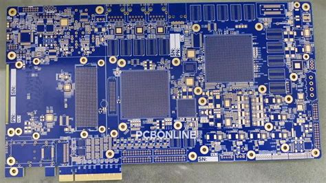
1.RF circuit board design
1.1 Layout of components
Since SMT generally uses infrared furnace hot flow soldering to achieve component welding, the layout of components affects the quality of solder joints, thereby affecting the yield of the product. As for RF circuit board design, electromagnetic compatibility requires that each circuit module should not generate electromagnetic radiation as much as possible, and have a certain ability to resist electromagnetic interference. Therefore, the layout of components also affects the interference and anti-interference ability of the circuit itself, which is directly related to the performance of the designed circuit. Therefore, in addition to considering the layout of general PCB design when designing RF circuit boards, it is also necessary to consider how to reduce the mutual interference between the various parts of the RF circuit, how to reduce the interference of the circuit itself to other circuits, and the anti-interference ability of the circuit itself.
According to experience, the performance of the RF circuit depends not only on the functional objectives of the RF circuit board itself, but also largely on the mutual influence between the CPU processing board. Therefore, when designing RF circuit boards, reasonable layout is particularly important. The general principle of layout is that the components should be placed in the same direction as much as possible, and the direction of the PCB board entering the tin melting system can be selected to reduce or even prevent poor welding; according to experience, there must be at least 0.5mm between the components to meet the tin melting requirements of the components. If the space of the PCB board allows, the distance between the components should be as wide as possible. For double-sided boards, one side should generally be designed for SMD and SMC components, and the other side for discrete components.
Things to note in RF PCB layout:
① First confirm the position of the interface components with other PCBs or systems on the PCB (RF PCB), and pay attention to the coordination issues between the interface components (the direction of the components, etc.);
② Group the unit circuits according to the different levels of electromagnetic compatibility sensitivity during use.
When arranging the components that are susceptible to interference in the circuit, the interference source should be avoided as much as possible (such as interference from the CPU on the data processing board);
③ Since the size of handheld devices is very small, the components are placed very compactly, so for the components with larger volume, it is necessary to give priority to them, confirm the corresponding position, and consider the cooperation between them;
④ Carefully analyze the circuit structure, divide the circuit into blocks (add high-frequency expansion circuit, mixing circuit and demodulation circuit, etc.), separate the strong electric signal and weak electric signal as much as possible, separate the digital signal circuit and the analog signal circuit, and the circuit that completes the same function should be arranged within a certain scale as much as possible, so as to reduce the signal loop area; the filtering network of each part of the circuit must be connected nearby, which can not only reduce radiation, but also reduce the probability of being interfered with, and improve the anti-interference ability of the circuit.
1.2 Wiring
After the layout of the components is basically completed, the wiring can be started. The basic principle of wiring is: when the assembly density allows, try to use low-density wiring planning, and the signal lines should be as thick and thin as possible, which is conducive to impedance matching.
For RF circuits, unreasonable planning of the direction, width, and line spacing of signal lines may cause cross-interference between signal transmission lines; in addition, the system power supply itself also has noise interference, so when designing RF circuit boards, comprehensive considerations must be made and reasonable wiring must be made. When wiring, all lines should be about 2mm away from the border of the PCB board to prevent the risk of disconnection or disconnection during PCB manufacturing.
The power line should be as wide as possible to reduce the loop resistance, and at the same time, the direction of the power line and the ground line should be consistent with the direction of data transmission to improve the anti-interference ability; the signal line should be as short as possible, and the number of vias should be minimized; the connection between the components should be as short as possible to reduce the distribution parameters and the electromagnetic interference between each other; incompatible signal lines should be kept as far away from each other as possible, and parallel routing should be avoided as much as possible, and the signal lines on the front and back sides should be perpendicular to each other; when wiring, the angle should be 135° where a corner is required to avoid turning a right angle.
When wiring, the lines directly connected to the pad should not be too wide, and the routing should be kept as far away from unconnected components as possible to prevent short circuits; vias should not be drawn on components, and should be kept as far away from unconnected components as possible to prevent the occurrence of cold soldering, continuous soldering, short circuits, etc. in the production of high-frequency microwave RF circuit boards. In the design of RF circuit boards, the correct wiring of power lines and ground lines is particularly important, and reasonable design is the most important means to defeat electromagnetic interference.
Quite a lot of interference sources on PCB boards are generated through power supply and ground wire,
among which the noise interference caused by ground wire is the largest. The main reason why ground wire easily causes electromagnetic interference is that there is impedance in ground wire. When current flows through the ground wire, voltage will be generated on the ground wire, and then ground wire loop current will be generated, forming loop interference of ground wire. When multiple circuits share a ground wire, common impedance coupling will be formed, and then the so-called ground wire noise will be generated.
Therefore, when wiring the ground wire of RF circuit board, the following should be done:
① When processing the circuit in blocks, the RF circuit can basically be divided into high-frequency extension, mixing, demodulation, local oscillation and other parts. A common potential reference point should be provided for each circuit module, that is, the ground wire of each module circuit, so that the signal can be transmitted between different circuit modules. Then, it is summarized at the place where the RF circuit board is connected to the ground wire, that is, it is summarized at the total ground wire. Since there is only one reference point, there is no common impedance coupling, and then there is no mutual interference problem;
② The digital area and the analog area should be isolated by ground wire as much as possible, and the digital ground and the analog ground should be separated and finally connected to the power ground;
③ The ground wire inside each part of the circuit should also pay attention to the single-point grounding principle, minimize the signal loop area, and connect it to the ground wire of the corresponding filter circuit as close as possible;
④ If space permits, it is best to isolate each module with a ground wire to prevent signal coupling effects between each other.


