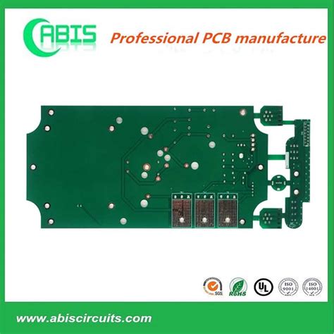
How to solve the problem of too many vias on PCB
Too many vias on PCB is a common problem in electronic design, which may be caused by many factors, such as unreasonable design, complex routing, signal requirements, etc. To solve the problem of too many vias on PCB, we need to start from multiple aspects such as design, layout, routing and communication with manufacturers.
I. Problem Analysis
1.1 The role and impact of vias
Via is a component used to connect lines between different layers on PCB. It changes the circuit board from a planar structure to a three-dimensional structure, improving the flexibility of design and the connectivity of the circuit. However, too many vias may bring the following problems:
Signal attenuation: Vias will introduce additional resistance, inductance and capacitance, causing attenuation of high-speed signal transmission.
Interference and coupling: The electromagnetic field interaction between vias may cause signal interference and coupling.
Increased manufacturing cost: Too many vias will increase the difficulty and cost of PCB manufacturing.
Reduced reliability: Vias are the weak link of PCB. Too many or too dense vias may reduce the reliability of the circuit board.
1.2 Reasons for too many vias
Irrational design: If the routing is not properly planned, some signals need to be connected by drilling and changing layers.
Functional requirements: Some special functions (such as high-speed signal transmission, high-density layout, high-power heat dissipation, etc.) require more vias.
Manufacturing restrictions: Some manufacturing processes or equipment may limit the number and layout of vias.

2.Solutions
2.1 Optimize the design
2.1.1 Merge components with similar functions
During the design process, you can consider merging components with similar functions, such as merging multiple capacitors or resistors of the same type into one component to reduce the number of vias required. This method not only reduces vias, but also simplifies the circuit layout and improves the compactness of the design.
2.1.2 Use SMD devices
Prefer surface mount devices (SMD) rather than through-hole devices. The characteristic of SMD devices is that they do not require vias. By reasonably selecting the layout and wiring of SMD devices, the overall number of vias can be significantly reduced. At the same time, SMD devices also have the advantages of small size, light weight, and easy automated production.
2.2 Adjust via types
2.2.1 Use blind and buried vias
Blind and buried vias are two special types of vias that can reduce the space occupied on the PCB surface and reduce the impact on signal integrity. Blind vias are drilled only on one side of the board, while buried vias are drilled inside the board and neither end is exposed. Whenever possible, try to use blind and buried vias to reduce the number of vias.
2.2.2 Embedded component technology
Embedded component technology embeds components directly into the internal layers of the PCB board, avoiding connections through vias. This technology can significantly reduce the number of vias and improve the reliability and stability of the circuit board. However, it should be noted that embedded component technology requires specialized manufacturing processes and equipment support, and is costly.
2.3 Optimize layout and routing
2.3.1 Compact layout
The number of vias can be reduced by optimizing the layout of components and arranging them as compactly as possible. Avoid excessive gaps and unnecessary crossings to reduce the need for vias. Compact layout also helps improve the heat dissipation performance and mechanical strength of the circuit board.
2.3.2 Interlayer connection
Consider using interlayer connection instead of connecting through vias. By using internal layers or traces for signal transmission, the need for vias in external layers can be reduced. This method is particularly suitable for multilayer board design and can significantly improve the flexibility of the design and the connectivity of the circuit.
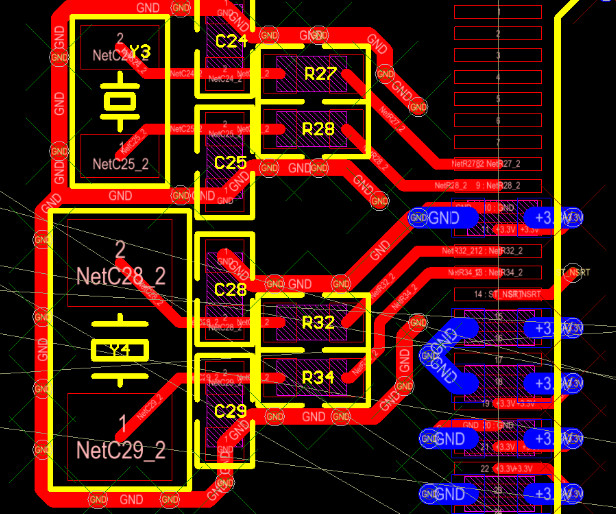
2.3.3 Reasonable routing planning
Reasonable routing planning is also an important means to reduce the number of vias. During the wiring process, unnecessary routing crossings and layer changes should be avoided as much as possible to reduce the use of vias. At the same time, attention should also be paid to keeping the routing neat and consistent to improve the stability and reliability of signal transmission.
2.4 Communicate with manufacturers
2.4.1 Understand manufacturing limitations
Before designing, it is necessary to communicate with manufacturers to understand their manufacturing capabilities and limitations. Manufacturers can provide best practices and suggestions on vias to help engineers optimize designs. By understanding manufacturing limitations, problems such as too many vias or unreasonable layouts can be avoided during the design process.
2.4.2 Manufacturing optimization suggestions
In order to improve yield and manufacturing efficiency, manufacturers usually provide manufacturing optimization suggestions. These suggestions may include using stacked holes, blind holes and other technologies to reduce the number of vias, or improving manufacturing processes and equipment to reduce manufacturing costs. Close communication with manufacturers can ensure the feasibility and economy of the design.
3. Detailed strategies and implementation steps
3.1 Detailed strategies
3.1.1 Refinement in the design stage
Layer planning: In the early stages of design, carefully plan the layering of the PCB. Clarify which layers are used for signal transmission, which layers are used for power and ground, and which layers may require special via processing. Through reasonable layer planning, unnecessary vias can be reduced and the transmission efficiency of signals can be improved.
Signal integrity analysis: Use professional signal integrity analysis tools (such as HFSS, ADS, etc.) to simulate and analyze the design. Through simulation, the transmission behavior of the signal on the PCB board can be predicted, including attenuation, reflection, crosstalk, etc., so that problems can be found and optimized in the design stage. This helps to reduce the number of vias increased due to signal integrity problems.
Modular design: Divide the complex circuit into several functional modules, and try to keep the routing simple and the vias as few as possible in each module. Modules are connected through standardized interfaces, which not only reduces the number of vias, but also improves the maintainability and scalability of the design.
3.1.2 Selection of manufacturing process
Advanced manufacturing technology: Consider using advanced manufacturing technology to reduce the number of vias. For example, microvia technology can achieve smaller via diameters and higher via density without increasing PCB thickness; laser drilling technology can achieve high-precision blind and buried via processing.
Flexible PCB: For application scenarios that require high flexibility and reduce the number of vias, consider using flexible PCB (FPC). Flexible PCB can be bent and folded, thus avoiding some vias that have to be used due to space constraints.
3.1.3 Cost control and performance balance
Cost-benefit analysis: While reducing the number of vias, a cost-benefit analysis should be performed. Although reducing vias can reduce manufacturing costs and improve performance, the introduction of certain technologies (such as blind and buried vias) may increase the complexity of manufacturing costs. Therefore, it is necessary to find the best balance between performance and cost.
Alternative solution evaluation: For some application scenarios where the number of vias cannot be reduced through design optimization, alternative solutions can be considered. For example, use high-performance connectors or cables to replace the via connections on some PCBs; or use a distributed power supply system to reduce the number of power vias.
3.2 Implementation steps
3.2.1 Demand analysis and design planning
Demand analysis: Communicate with customers or project teams to clarify the functional requirements and performance indicators of the circuit board. Including signal transmission rate, power consumption, heat dissipation requirements, cost budget, etc.
Design planning: According to the results of demand analysis, make a detailed design plan. Including selecting appropriate PCB materials, number of layers, size and thickness; determining the layout and routing strategy of components; planning the type, number and location of vias, etc.
3.2.2 Layout and wiring
Layout design: Design the layout of components according to the design plan. Follow the principles of compactness, order and easy maintenance for layout. At the same time, pay attention to avoid interference and conflict between components.
Wiring design: Perform wiring design after the layout is determined. Try to use straight lines or 45-degree angles for wiring, and avoid using too many arcs and broken lines. At the same time, pay attention to the width, spacing, and interlayer connection strategy of the routing to reduce unnecessary vias.
3.2.3 Simulation analysis and optimization
Signal integrity simulation: Use simulation tools to perform signal integrity simulation analysis on the design. Including S parameter simulation, time domain reflection simulation, etc. Use simulation results to evaluate the performance of the design and find potential problems.
Optimize design: Optimize the design according to the simulation results. Adjust component layout, routing strategy, and via position, etc. to improve signal transmission efficiency and reduce the number of vias. At the same time, pay attention to maintaining the compactness and maintainability of the design.
3.2.4 Manufacturing and testing
Communicate with manufacturers: Submit the design files to the manufacturer and communicate with them about the manufacturing process and restrictions. Adjust and optimize the design according to the manufacturer’s suggestions.
Manufacturing: The manufacturer manufactures the PCB according to the design files. Including process steps such as cutting, drilling, electroplating, and etching. Pay attention to controlling quality and cost during the manufacturing process.
Test verification: Test and verify the produced PCB boards. Including electrical performance test, signal integrity test and environmental adaptability test, etc. Test to verify the correctness and reliability of the design and find potential problems.
Problem rectification: If problems are found during the test, the design needs to be rectified. Modify and optimize the design according to the test results and problem feedback, and re-manufacture and test.
3.2.5 Maintenance and upgrade
Maintenance and care: Regular maintenance and care of PCB boards during use. Including cleaning, heat dissipation, moisture-proof and other measures. To extend the service life of PCB boards and improve their reliability.
Upgrade and improvement: With the continuous development of technology and changes in application requirements, PCB boards need to be upgraded and improved. Including updating components, optimizing layout and wiring, introducing new technologies, etc. To improve the performance of circuit boards and meet new application requirements.
IV. Advanced strategies and application cases
4.1 Advanced strategies
4.1.1 3D packaging technology
With the continuous advancement of semiconductor technology, 3D packaging technology has gradually become an important means to solve PCB via problems. 3D packaging technology greatly reduces the number of vias on PCB boards by stacking multiple chips or components vertically and connecting them through micro-vias (TSV, Through Silicon Via) or micro-bumps. This technology not only improves the integration of circuits, but also significantly improves signal transmission performance and power consumption.
4.1.2 High-speed signal transmission technology
For the needs of high-speed signal transmission, differential signals, low-loss materials, impedance matching and other technologies can be used to optimize PCB design, reduce signal attenuation and interference, and thus reduce dependence on vias. For example, by accurately controlling the width, spacing and interlayer dielectric thickness of the traces, good impedance matching can be achieved, signal reflection and crosstalk can be reduced; using low-loss PCB materials can reduce energy loss during signal transmission.
4.1.3 Intelligent design tools
Using intelligent design tools, such as AI-assisted design software, PCB layout and routing can be automatically optimized to reduce the number of vias. These tools use algorithms to analyze the functions and performance requirements of the circuit, and automatically adjust the component position, routing strategy and via position to achieve the best design effect. Intelligent design tools can not only improve design efficiency, but also reduce the risk of human error.
4.2 Application Cases
Case 1: High-speed communication board design
In the design of high-speed communication boards, a large number of vias and dense distribution is a common problem. To solve this problem, the design team adopted differential signal transmission, low-loss materials and impedance matching technology. By precisely controlling the routing parameters and selecting suitable PCB materials, signal attenuation and interference were successfully reduced, and the number of vias was reduced. At the same time, the layout and wiring were optimized using intelligent design tools, further improving the reliability and performance of the design.
Case 2: Automotive radar system PCB design
The automotive radar system has extremely high performance requirements for PCBs, especially the stability and reliability of signal transmission. In order to reduce the number of vias and improve the quality of signal transmission, the design team used 3D packaging technology to stack key chips vertically and connect them through micro-vias. This design not only greatly reduces the number of vias on the PCB board, but also improves the signal transmission speed and anti-interference ability. In addition, the design team also reduced electromagnetic radiation and noise interference by optimizing the layout of the power and ground networks, ensuring the stable operation of the radar system.
Case 3: PCB Design of Medical Electronic Equipment
Medical electronic equipment has extremely high requirements for the reliability and safety of PCBs. In order to reduce the number of vias and improve the reliability of the design, the design team adopted a modular design strategy. They divided the circuit into multiple functional modules and carried out detailed layout and routing inside each module. At the same time, the number of vias was further reduced by using high-performance connectors and cables to replace the via connections on some PCBs. In addition, the design team also conducted rigorous reliability testing and verification of the PCB to ensure the stable operation of medical equipment in harsh environments.
5.Conclusion and Outlook
The problem of too many vias on PCB boards is a complex and important challenge, which involves circuit design, manufacturing process, performance optimization and other aspects. By adopting strategies such as optimized design, adjusting via types, optimizing layout and routing, communicating with manufacturers, and introducing new technologies, we can effectively reduce the number of vias and improve the performance and reliability of PCBs. In the future, with the continuous development of electronic technology and the advancement of manufacturing processes, we have reason to believe that PCB design will become more efficient, intelligent and reliable. At the same time, we also need to keep an eye on the development of new technologies and new materials so that we can apply them to PCB design in a timely manner to promote the continuous progress and development of the electronics industry.