How to Successfully Design and Manufacture High-Complexity PCBs and PCBAs
Introduction
Printed Circuit Boards (PCBs) and Printed Circuit Board Assemblies (PCBAs) are the backbone of modern electronics. As technology advances, the demand for high-complexity PCBs and PCBAs continues to grow. These boards are found in applications such as aerospace, medical devices, telecommunications, and high-performance computing, where reliability, precision, and performance are critical.
Designing and manufacturing high-complexity PCBs and PCBAs requires a deep understanding of electrical engineering, material science, thermal management, and manufacturing processes. This article explores best practices for successfully developing high-complexity PCBs and PCBAs, covering design considerations, material selection, manufacturing challenges, and quality assurance.
1. Key Considerations in High-Complexity PCB Design
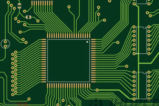
1.1. Advanced Schematic Design and Layout Planning
Before starting the PCB layout, a well-structured schematic is essential. High-complexity PCBs often involve:
- High-speed digital signals (DDR, PCIe, USB 4.0)
- RF/microwave circuits (5G, radar systems)
- Mixed-signal designs (analog + digital)
- Power integrity challenges (high-current power delivery networks)
Best Practices:
- Use hierarchical schematics for better organization.
- Define clear signal paths and critical net classes.
- Simulate signal integrity (SI) and power integrity (PI) early in the design phase.
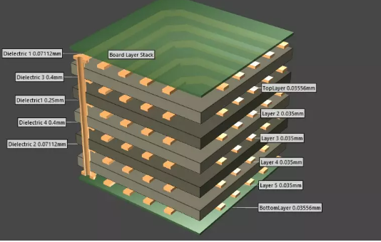
1.2. Layer Stackup and Impedance Control
High-complexity PCBs often require multilayer stackups (12+ layers) with controlled impedance for high-speed signals.
Key Factors:
- Dielectric materials (FR4, Rogers, Isola) must match signal frequency requirements.
- Impedance matching (differential pairs, single-ended traces) must be calculated and verified.
- Via optimization (blind/buried vias, microvias for HDI designs).
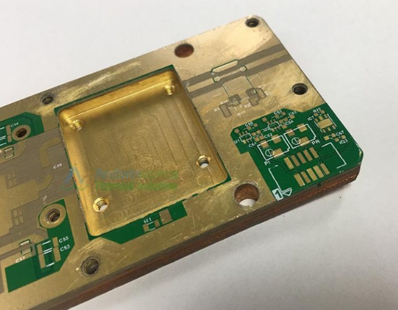
1.3. Thermal Management
High-power components (CPUs, FPGAs, GPUs) generate significant heat, requiring:
- Thermal vias to dissipate heat.
- Copper pours and heatsinks for better thermal conductivity.
- Simulation tools (ANSYS, Cadence Celsius) to predict thermal performance.
1.4. EMI/EMC Considerations
Electromagnetic interference (EMI) can degrade performance. Mitigation techniques include:
- Proper grounding strategies (star grounding, ground planes).
- Shielding (Faraday cages, conductive coatings).
- Careful routing (avoiding parallel high-speed and sensitive analog traces).
2. Material Selection for High-Complexity PCBs
The choice of materials impacts performance, reliability, and manufacturability.
2.1. Substrate Materials
- Standard FR4: Cost-effective but limited for high-frequency applications.
- High-Tg FR4: Better thermal stability for lead-free soldering.
- Rogers & PTFE-based laminates: Low-loss materials for RF/microwave designs.
2.2. Copper Foil Selection
- Electrodeposited (ED) copper: Standard for most PCBs.
- Rolled annealed (RA) copper: Better for flexible PCBs and high-frequency designs.
2.3. Surface Finishes
- ENIG (Electroless Nickel Immersion Gold): Good for fine-pitch components.
- OSP (Organic Solderability Preservative): Cost-effective but less durable.
- Immersion Silver: Suitable for high-frequency applications.
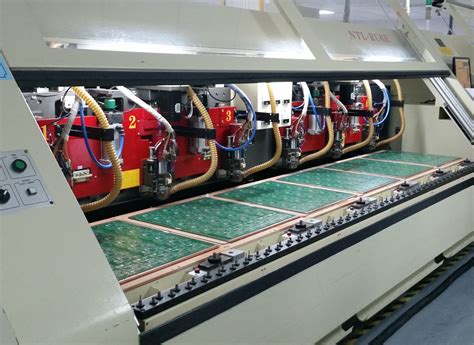
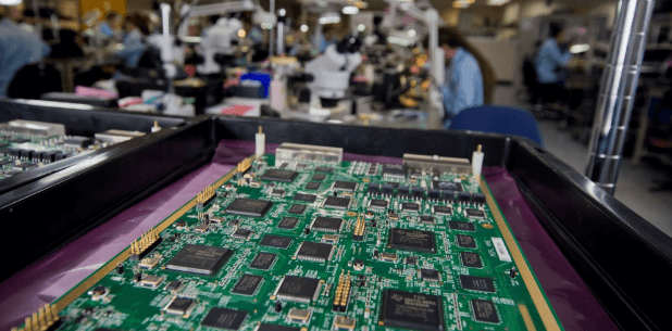
3. Manufacturing Challenges in High-Complexity PCBAs
3.1. Precision Fabrication Requirements
- Tighter tolerances (trace width/spacing ≤ 3/3 mil).
- Laser-drilled microvias for HDI designs.
- Advanced plating techniques (via filling, copper uniformity).
3.2. Assembly Challenges
- Fine-pitch components (BGA, QFN, 01005 passives) require high-precision placement.
- Mixed-technology assembly (through-hole + SMT + press-fit connectors).
- Reflow soldering profiles must be optimized to avoid tombstoning or voiding.
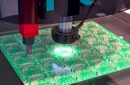
3.3. Testing and Inspection
- Automated Optical Inspection (AOI): Detects soldering defects.
- X-ray inspection: Essential for BGA and hidden solder joints.
- In-Circuit Testing (ICT): Validates electrical functionality.
4. Quality Assurance and Reliability Testing
High-complexity PCBAs must undergo rigorous testing:
4.1. Environmental Stress Testing
- Thermal cycling (-40°C to +125°C).
- Vibration and shock testing (MIL-STD-810).
- Humidity resistance (85°C/85% RH).
4.2. Long-Term Reliability
- HALT (Highly Accelerated Life Testing) identifies weak points.
- MTBF (Mean Time Between Failures) analysis predicts lifespan.
5. Future Trends in High-Complexity PCBs/PCBAs
- Embedded components (resistors, capacitors inside the PCB).
- Additive manufacturing (3D-printed electronics).
- AI-driven design optimization for better performance.
Conclusion
Designing and manufacturing high-complexity PCBs and PCBAs is a multidisciplinary challenge that requires expertise in electrical engineering, materials science, and advanced manufacturing techniques. By following best practices in design, material selection, fabrication, and testing, engineers can ensure reliable, high-performance PCBAs for cutting-edge applications.
As technology evolves, staying updated with the latest trends and innovations will be crucial for success in this demanding field.