How to Test the Extreme Temperature Limits of PCB Boards
Introduction
Printed Circuit Boards (PCBs) form the backbone of modern electronics, and their performance under extreme temperature conditions is critical for many applications. From aerospace systems that experience cryogenic temperatures to industrial equipment operating near molten metals, understanding a PCB’s temperature limits is essential for reliability and safety. This article provides a comprehensive guide on testing PCB extreme temperature limits, covering test methodologies, equipment requirements, industry standards, and best practices.
Understanding PCB Temperature Limits
Before conducting extreme temperature tests, it’s important to understand what constitutes a PCB’s temperature limits:
- Maximum Operating Temperature: The highest temperature at which the PCB can function normally
- Minimum Operating Temperature: The lowest temperature at which the PCB maintains functionality
- Glass Transition Temperature (Tg): The point at which the substrate material changes from rigid to flexible
- Decomposition Temperature (Td): The temperature at which the PCB material begins to chemically decompose
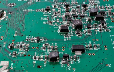
These limits vary significantly based on the PCB materials (FR-4, polyimide, ceramic, etc.), component selection, and manufacturing processes.
Test Preparation
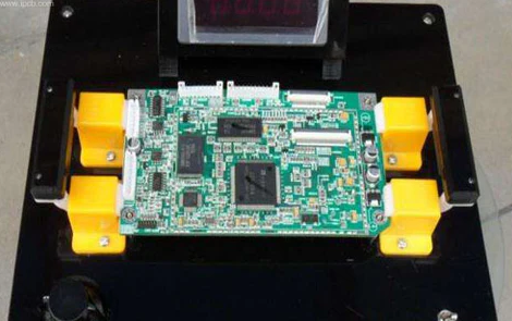
1. Sample Selection and Preparation
- Select representative production samples (minimum 5 boards recommended)
- Clean boards thoroughly to remove contaminants that might affect results
- Document initial conditions with high-resolution photographs
- Measure and record baseline electrical performance
2. Instrumentation Requirements
- High-precision temperature chambers capable of reaching target extremes
- Thermocouples or infrared thermometers for accurate temperature measurement
- Data acquisition system for continuous monitoring
- Insulation resistance test equipment
- Function generator and oscilloscope for signal integrity testing
Test Methodologies
1. Steady-State Temperature Testing
This method evaluates PCB performance at constant extreme temperatures:
- Place the PCB in the temperature chamber with appropriate fixturing
- Ramp temperature at ≤5°C/min to prevent thermal shock
- Maintain target temperature for a predetermined duration (typically 2-4 hours)
- Perform in-situ functional testing
- Cool at controlled rate and inspect for physical damage
2. Thermal Cycling Testing
Assesses the PCB’s ability to withstand repeated temperature variations:
- Program the chamber for repeated cycles between temperature extremes
- Typical cycle: -40°C to +125°C with 15-30 minute dwell times
- Perform electrical tests at room temperature after every 50-100 cycles
- Continue until failure or completion of specified cycles (often 500-1000)
3. Thermal Shock Testing
Evaluates resistance to sudden temperature changes:
- Use separate hot and cold chambers or a specialized thermal shock chamber
- Transfer boards rapidly between extremes (typically <1 minute)
- Dwell times of 5-15 minutes at each extreme
- Inspect after specified number of cycles (often 50-200)
4. Humidity-Temperature Bias Testing
Combines temperature extremes with humidity for more severe conditions:
- Maintain 85°C/85% RH or other specified conditions
- Apply operating voltage to the PCB during testing
- Typical duration: 96-1000 hours
- Monitor for electrochemical migration and insulation breakdown
Key Parameters to Measure
During extreme temperature testing, monitor these critical parameters:
- Electrical Continuity: Verify all circuits maintain proper connectivity
- Insulation Resistance: Measure between conductors and ground planes
- Dielectric Withstanding Voltage: Test for adequate isolation at high potentials
- Signal Integrity: Evaluate high-speed signals for distortion or attenuation
- Physical Deformation: Check for delamination, warping, or cracking
- Component Functionality: Verify all mounted components operate correctly
- Solder Joint Integrity: Inspect for cracks or separation
Industry Standards for Reference
Several established standards govern PCB temperature testing:
- IPC-TM-650: Standard test methods for printed boards
- IPC-6012: Qualification and performance specification for rigid PCBs
- MIL-STD-202: Electronic component test methods (including temperature)
- IEC 60068: Environmental testing standards
- JEDEC JESD22-A104: Temperature cycling standard
- ASTM D5483: Standard for dielectric withstand voltage testing
Safety Considerations
Extreme temperature testing presents several hazards:
- Personal Protection: Use insulated gloves and face protection when handling extreme temperature samples
- Chamber Safety: Ensure proper ventilation for high-temperature outgassing
- Electrical Isolation: Use appropriate insulation for in-situ testing
- Cryogenic Precautions: Special handling required for liquid nitrogen-cooled tests
- Failure Modes: Be prepared for potential fire hazards with overheated boards
Data Analysis and Reporting
Proper documentation is essential for meaningful results:
- Record all test parameters (temperatures, durations, ramp rates)
- Document all measurements with timestamps
- Photograph any physical changes or failures
- Analyze failure modes (location, mechanism, progression)
- Compare results against specifications and standards
- Generate comprehensive test reports including:
- Test conditions and procedures
- Raw data and observations
- Failure analysis
- Conclusions and recommendations
Advanced Testing Techniques
For more sophisticated analysis, consider these methods:
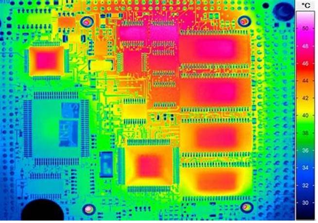
- Thermal Imaging: Identify hot spots and thermal distribution
- Microsectioning: Examine internal structure changes post-testing
- CT Scanning: Non-destructive internal inspection
- Dynamic Mechanical Analysis (DMA): Measure material property changes
- Thermogravimetric Analysis (TGA): Determine decomposition temperatures
Common Failure Modes at Temperature Extremes
Understanding potential failure mechanisms helps in test design:
High Temperature Failures:
- Delamination of layers
- Solder reflow or component detachment
- Conductive anodic filament (CAF) formation
- Substrate decomposition
- Copper creep and pad lifting
Low Temperature Failures:
- Brittle fracture of materials
- Solder joint cracking
- Condensation and icing issues
- Increased dielectric losses
- Component parameter drift
Optimizing PCB Design for Extreme Temperatures
Testing often reveals design improvements:
- Material selection (high-Tg laminates, ceramic substrates)
- Copper weight and distribution for thermal management
- Via design and plating for thermal cycling resistance
- Component placement considering thermal gradients
- Conformal coatings for environmental protection
- Thermal relief in pads and traces
Conclusion
Proper testing of PCB extreme temperature limits is a complex but essential process for ensuring reliability in harsh environments. By following systematic test methodologies, adhering to industry standards, and carefully analyzing results, engineers can accurately characterize PCB performance boundaries. This knowledge enables appropriate design decisions and helps prevent field failures in temperature-critical applications.
As electronics continue to expand into more extreme environments—from deep space to geothermal applications—the importance of thorough temperature limit testing will only grow. Implementing the rigorous testing approaches outlined in this article provides the data needed to push PCB technology to its limits while maintaining reliability.
Remember that temperature testing should be an iterative process, with findings from initial tests informing design improvements that are then validated through subsequent testing. This cyclical approach leads to robust PCB designs capable of withstanding even the most challenging thermal environments.