How to use double sided prototype pcb
Mastering Soldering Techniques on Double-Sided Prototype PCBs
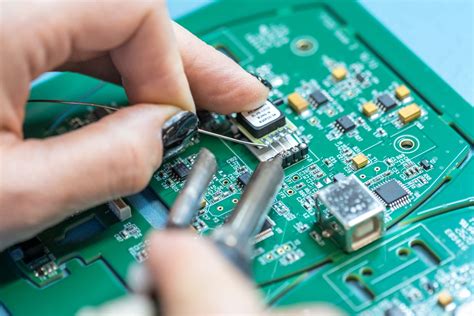
Mastering soldering techniques on double-sided prototype PCBs is an essential skill for electronics enthusiasts and professionals alike. Double-sided PCBs, which have conductive copper layers on both sides, offer increased circuit density and flexibility in design. However, they also present unique challenges that require careful attention and precision. To begin with, it is crucial to understand the layout and design of the double-sided PCB. This involves studying the schematic and layout diagrams to identify the placement of components and the routing of traces. Familiarity with the design will help in planning the soldering process and avoiding potential errors.
Before starting the soldering process, it is important to gather the necessary tools and materials.
A high-quality soldering iron with adjustable temperature control is essential for achieving clean and reliable solder joints. Additionally, using a fine-tipped soldering iron can help in accessing tight spaces on the PCB. Solder wire, preferably with a flux core, is needed to create the connections between components and the PCB. Flux is a chemical cleaning agent that helps remove oxidation from metal surfaces, ensuring a strong bond between the solder and the components.
Once the tools are ready, the next step is to prepare the PCB and components.
This involves cleaning the PCB to remove any dust, grease, or oxidation that may interfere with the soldering process. Isopropyl alcohol and a lint-free cloth can be used for this purpose. Similarly, the leads of the components should be cleaned to ensure good electrical contact. After cleaning, it is advisable to perform a dry fit by placing the components on the PCB without soldering them. This helps in verifying the correct placement and orientation of each component.
With the preparation complete, the soldering process can begin. It is important to start with the components that are mounted on the bottom side of the PCB.
This is because soldering components on the top side first can make it difficult to access the bottom side. When soldering, it is crucial to apply the right amount of heat and solder. Too much heat can damage the components or the PCB, while too little heat can result in weak solder joints. The soldering iron should be placed on the joint for just enough time to melt the solder and form a shiny, concave fillet around the lead and pad.
As the soldering progresses, it is important to periodically inspect the joints for quality.
A good solder joint should be smooth, shiny, and free of any gaps or voids. If any defects are found, they should be corrected immediately by reheating the joint and adding more solder if necessary. Once all the components on the bottom side are soldered, the PCB can be flipped over to solder the components on the top side. Care should be taken to avoid disturbing the already soldered joints on the bottom side.
Finally, after all the components are soldered, it is important to perform a thorough inspection and testing of the PCB. This involves checking for any solder bridges, cold joints, or other defects that may affect the performance of the circuit. Additionally, continuity testing can be performed using a multimeter to ensure that all connections are properly made. By following these steps and paying attention to detail, one can master the art of soldering on double-sided prototype PCBs, leading to successful and reliable electronic projects.
Designing Efficient Circuit Layouts on Double-Sided Prototype PCBs
Designing efficient circuit layouts on double-sided prototype PCBs requires a strategic approach to maximize the potential of the available space and ensure optimal functionality. Double-sided PCBs, which feature conductive pathways on both sides, offer increased flexibility and complexity in circuit design compared to their single-sided counterparts. This added layer of complexity, however, necessitates careful planning and execution to avoid common pitfalls such as signal interference and inefficient use of space.
To begin with, it is essential to have a clear understanding of the circuit requirements and the components involved.
This involves creating a schematic diagram that outlines the connections and interactions between different components. By doing so, one can identify the critical paths and components that need to be prioritized in the layout. Once the schematic is complete, the next step is to translate this into a physical layout on the PCB. This process involves placing components in a manner that minimizes the length of critical signal paths, thereby reducing potential signal degradation and interference.
When working with double-sided PCBs, it is crucial to make effective use of both sides of the board.
Typically, one side is designated for placing components, while the other is used for routing traces. This separation helps in reducing congestion and allows for more straightforward troubleshooting and modifications. However, it is not uncommon to place components on both sides, especially in more complex designs. In such cases, careful consideration must be given to the placement to ensure that components do not interfere with each other and that soldering can be performed efficiently.
Transitioning from component placement to trace routing, it is important to consider the use of vias, which are small conductive holes that allow signals to pass between the two layers of the PCB.
Vias are instrumental in connecting traces on different sides of the board, but they should be used judiciously. Excessive use of vias can lead to increased manufacturing costs and potential reliability issues. Therefore, it is advisable to plan the routing in such a way that minimizes the need for vias while still maintaining efficient signal paths.
Another critical aspect of designing on double-sided PCBs is managing power distribution and grounding.
A well-designed power distribution network ensures that all components receive the necessary power without significant voltage drops. Similarly, a robust grounding strategy is essential to prevent noise and interference from affecting the circuit’s performance. Often, one side of the PCB is dedicated to a ground plane, which provides a common return path for current and helps in reducing electromagnetic interference.
In addition to these technical considerations, it is also important to keep in mind the practical aspects of PCB design, such as manufacturability and testing.
Ensuring that the design adheres to standard manufacturing processes can help in reducing production costs and lead times. Furthermore, incorporating test points and considering the ease of access for testing equipment can facilitate efficient troubleshooting and validation of the circuit.
In conclusion, designing efficient circuit layouts on double-sided prototype PCBs involves a careful balance of technical and practical considerations. By strategically placing components, optimizing trace routing, and managing power distribution, one can create a functional and reliable PCB design. With thoughtful planning and execution, double-sided PCBs can offer significant advantages in terms of complexity and performance, making them an invaluable tool in the development of modern electronic devices.
Troubleshooting Common Issues with Double-Sided Prototype PCBs
When working with double-sided prototype PCBs, troubleshooting common issues is an essential skill for ensuring the functionality and reliability of your electronic projects. Double-sided PCBs, which feature conductive pathways on both sides, offer increased circuit density and complexity, making them a popular choice for many applications. However, this complexity can also lead to a range of potential issues that require careful attention and methodical troubleshooting.
One of the most frequent problems encountered with double-sided PCBs is poor soldering, which can result in weak connections or even open circuits.
To address this, it is crucial to inspect all solder joints meticulously. Using a magnifying glass or a microscope can help identify cold solder joints, which appear dull and grainy, as opposed to the shiny and smooth appearance of a proper solder joint. Reflowing the solder with a soldering iron can often resolve these issues, ensuring a solid connection between components and the PCB.
Another common issue is the misalignment of vias, which are small holes that allow electrical connections between the two sides of the PCB.
Misaligned vias can disrupt the intended electrical pathways, leading to circuit failures. To troubleshoot this, verify the alignment of the vias during the design phase using PCB design software. If misalignment is detected after fabrication, it may be necessary to manually adjust the vias or use conductive ink to restore the connection.
In addition to soldering and via alignment, component placement errors can also pose significant challenges.
Double-sided PCBs offer the advantage of placing components on both sides, but this can lead to confusion and mistakes during assembly. To mitigate this, it is advisable to use a clear and detailed assembly guide, marking the positions of each component on both sides of the PCB. Cross-referencing the physical board with the schematic diagram can help ensure that all components are correctly placed and oriented.
Furthermore, electrical shorts are a common issue that can arise from improper handling or design flaws.
Shorts occur when unintended connections form between conductive traces, leading to circuit malfunctions. To identify shorts, a multimeter can be used to test for continuity between traces that should not be connected. If a short is detected, carefully inspect the PCB for solder bridges or debris that may be causing the connection. Removing excess solder or cleaning the board can often resolve these issues.
Thermal management is another critical aspect to consider when troubleshooting double-sided PCBs.
Overheating can lead to component failure and reduced lifespan of the PCB. Ensuring adequate heat dissipation through the use of heat sinks, thermal vias, or appropriate spacing between components can help prevent thermal-related issues. Monitoring the temperature of the PCB during operation can also provide insights into potential thermal problems.
Finally, it is important to consider the quality of the PCB material itself.
Low-quality materials can lead to issues such as delamination or warping, which can affect the overall performance of the board. Selecting high-quality materials and working with reputable manufacturers can help mitigate these risks.
In conclusion, troubleshooting double-sided prototype PCBs involves a comprehensive approach that addresses soldering quality, via alignment, component placement, electrical shorts, thermal management, and material quality. By systematically addressing these common issues, you can enhance the reliability and functionality of your double-sided PCBs, ensuring successful electronic projects.
Optimizing Component Placement on Double-Sided Prototype PCBs
When working with double-sided prototype PCBs, optimizing component placement is crucial for ensuring both functionality and manufacturability. The process begins with a thorough understanding of the circuit design and the specific requirements of the project. By carefully considering the layout, engineers can minimize potential issues such as signal interference, thermal management challenges, and manufacturing difficulties. To achieve an optimal layout, it is essential to follow a systematic approach that incorporates strategic planning and attention to detail.
Initially, it is important to categorize components based on their function and electrical characteristics.
Grouping similar components together can simplify routing and reduce the complexity of the design. For instance, placing all power-related components in one area can help in managing power distribution efficiently. Similarly, grouping analog and digital components separately can minimize noise interference, which is particularly crucial in mixed-signal designs.
Once components are categorized, the next step is to determine the most suitable side of the PCB for each group. Typically, larger and heavier components, such as transformers or heat sinks, are placed on the top side to provide better mechanical support and heat dissipation. Conversely, smaller and lighter components can be placed on the bottom side, taking advantage of the additional space available on a double-sided board.
Transitioning to the next phase, engineers must consider the placement of connectors and interfaces.
These components should be positioned in a manner that facilitates easy access and connection to external devices. Aligning connectors along the edges of the PCB can simplify assembly and improve the overall usability of the device. Furthermore, it is advisable to place test points and debugging interfaces in accessible locations to facilitate troubleshooting and testing during the prototyping phase.
As the design progresses, attention must be paid to the routing of traces.
Efficient routing is essential to maintain signal integrity and reduce electromagnetic interference. To achieve this, engineers should aim to keep trace lengths as short as possible and avoid unnecessary bends or vias. When routing on a double-sided PCB, it is beneficial to use one side primarily for horizontal traces and the other for vertical traces. This orthogonal routing strategy can help in reducing crosstalk and simplifying the overall layout.
Thermal management is another critical aspect to consider when optimizing component placement.
Components that generate significant heat should be placed in areas with adequate airflow or near heat sinks to prevent overheating. Additionally, thermal vias can be used to transfer heat from one side of the PCB to the other, enhancing the board’s overall thermal performance.
Finally, manufacturability should always be a key consideration in the design process.
Ensuring that components are placed with sufficient spacing can prevent soldering issues and improve the reliability of the final product. It is also important to adhere to the design rules and guidelines provided by the PCB manufacturer to avoid potential production delays or defects.
In conclusion, optimizing component placement on double-sided prototype PCBs requires a careful balance of electrical, mechanical, and thermal considerations. By systematically categorizing components, strategically placing connectors, efficiently routing traces, and addressing thermal management, engineers can create a robust and reliable PCB design. This meticulous approach not only enhances the performance of the prototype but also facilitates a smoother transition to mass production.


