How to use single-sided PCB to achieve wiring impedance control
You will probably think like this:
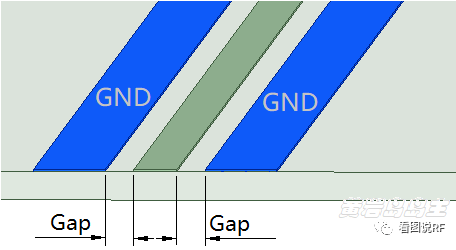
Single-sided PCB, without ground plane, can achieve wiring impedance control by using coplanar waveguide structure with ground wires on both sides:
It’s a beautiful idea, full of theory, but skinny in reality.
The boss who can think of using single-sided PCB to achieve wiring impedance control must have considered the extreme in material cost:
Compared with conventional double-sided PCB, single-sided PCB has fewer processes such as via metallization, back copper etching, back silk screen, back green oil, etc., which reduces the PCB manufacturing cost;
The single-sided wiring area will also be minimized as much as possible. Laying the ground on both sides increases the wiring area and the difficulty of wiring, so the ground can only be laid on one side (following the ground wire).
So, the impedance of single-sided grounding is determined by the size of the grounding gap?
That’s naive again, typical of not being tortured by society.
The boss who can think of single-sided wiring impedance control will definitely find a very low-cost three-wire PCB manufacturer for processing. Don’t expect the line width (equivalent to the line gap) processing accuracy. This kind of three-wire PCB manufacturer only guarantees basic continuity.
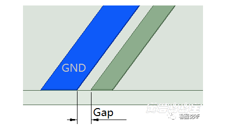
Relationship between the gap and impedance of single-sided grounding
In order to make everyone give up, HFSS modeling is specially used, FR4 medium thickness 20mil, copper thickness 1.4mil, line width 30mil. Take a look at the relationship between the Gap and impedance of the single-sided ground:
Take a look at the relationship between the Gap and impedance of the single-sided ground:
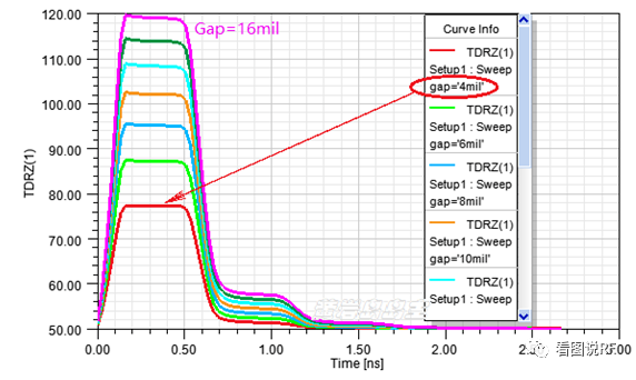
30mil line width single-sided wiring, copper gap Gap = 4mil (the copper gap that can be processed by the ordinary manufacturing process of mainstream PCB manufacturers), the impedance can only be 77 ohms, which is far from 50 ohms.
Copper gap Gap = 4mil is probably the copper gap that mainstream PCB manufacturers can guarantee the switching capability. The actual processed Gap may be in the range of 3~5mil. It is normal to have an error of +/-1mil, which will cause the impedance control error to exceed 20%.
Even so, don’t expect low-cost third-rate PCB manufacturers to process 4mil copper gaps.
The purple line in the above figure corresponds to the copper gap Gap=16mil.
Solution
According to the formula Z0 = sqrt (L0/C0), increasing the capacitance per unit length can reduce the impedance to 50 ohms.
Unit length refers to the length that is much smaller than the wavelength of the waveguide.
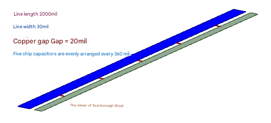
The capacitance per unit length is achieved by using evenly arranged chip capacitors.
The model below:
The simulated impedance is as follows:
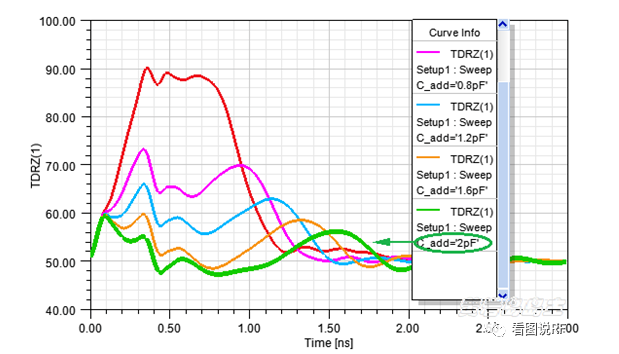
The red line is 0.4pF, and the TDR curve shows an impedance of 88 ohms;
The green line is 2pF, and the TDR curve is closest to 50 ohms;
This means that for this wiring structure with a length of 2000mil, a total of 5*2 = 10pF of additional capacitance needs to be added with chip capacitors to reduce the impedance to about 50 ohms.
Take a look at the return loss:
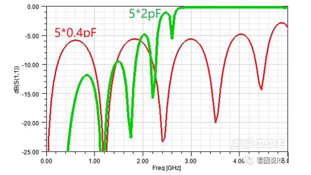
For digital circuits, assuming the return loss is limited to 10dB:
5*2pF topology can roughly transmit 1Gbps signal.
5*0.4pF topology can roughly transmit 0.15Gbps signal.
Still have gains.
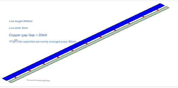
Unit length halved
Model below:
Take a look at the TDR instantaneous impedance of the topology above, and its relationship with the rising edge Tr:
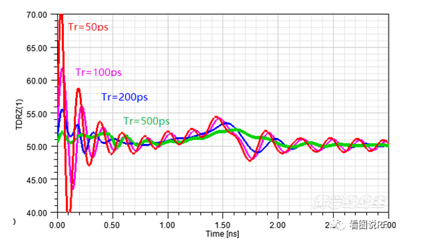
The blue line impedance is roughly controlled at +/-10%, corresponding to the rise time Tr=200ps.
The green line impedance is roughly controlled at +/-5%, corresponding to a rise time of Tr=500ps.
Let’s take a look at the return loss:
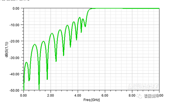
According to the previously assumed standard, 1pF capacitors are placed every 180mil, which can roughly transmit 2.2Gbps data signals.
The model in this article uses the LumpRLC boundary condition of HFSS, which still has differences in distributed parameters from actual patch components, and the error is not large at low frequencies.
Summary
The coplanar waveguide structure can theoretically achieve 50-ohm impedance control for single-sided PCB wiring, but it is difficult to achieve in actual engineering: because the copper spacing Gap is required to be less than 4mil.
A large copper spacing Gap=20mil can be used, but the patch capacitors are placed every unit length to achieve 50-ohm impedance control:
A 2pF capacitor is placed every 360mil, which can roughly transmit 1Gbps data signals.
If 1pF capacitors are placed every 180mil, 2Gbps data signals can be transmitted.
And so on.
The capacitor spacing cannot be smaller than the package body, right? Therefore, this topology can only be used for low-frequency and low-speed signals.