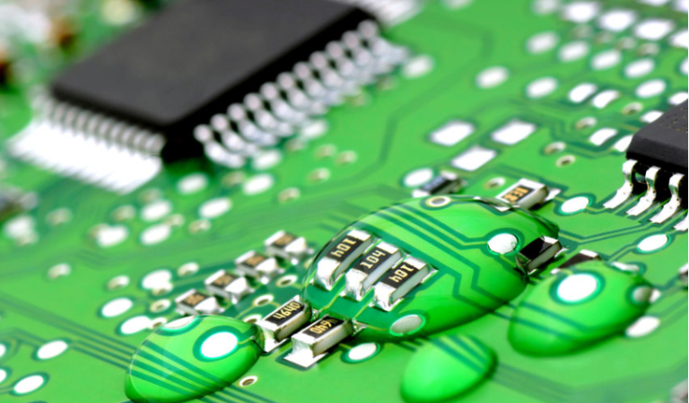
Immersion gold high-frequency pcb
Advantages Of Immersion Gold In High-Frequency PCB Design
Immersion gold, a popular surface finish in the realm of printed circuit boards (PCBs), offers a multitude of advantages, particularly in high-frequency PCB design. As electronic devices continue to evolve, the demand for high-frequency applications has surged, necessitating the use of materials and finishes that can meet stringent performance requirements. Immersion gold, known for its excellent conductivity and reliability, emerges as a preferred choice for engineers and designers working on high-frequency PCBs.
One of the primary advantages of immersion gold in high-frequency PCB design is its superior electrical conductivity.
Gold, being an excellent conductor, ensures minimal signal loss, which is crucial in high-frequency applications where even the slightest impedance can lead to significant performance degradation. This characteristic is particularly beneficial in applications such as telecommunications, aerospace, and advanced computing, where maintaining signal integrity is paramount. Furthermore, the thin layer of gold deposited during the immersion process provides a smooth and uniform surface, which is essential for consistent signal transmission across the PCB.
In addition to its conductivity, immersion gold offers remarkable corrosion resistance.
High-frequency PCBs are often exposed to harsh environmental conditions, including humidity and temperature fluctuations, which can lead to oxidation and corrosion of the conductive traces. The gold layer acts as a protective barrier, preventing oxidation and ensuring the longevity of the PCB. This durability is especially important in applications where reliability and long-term performance are critical, such as in military and medical devices.
Moreover, immersion gold provides excellent solderability, which is a significant advantage during the assembly process.
The smooth and even surface finish facilitates easy soldering, reducing the likelihood of defects such as poor wetting or non-wetting. This not only enhances the overall quality of the PCB but also streamlines the manufacturing process, leading to cost savings and increased efficiency. The ability to produce high-quality solder joints is particularly important in high-frequency applications, where any imperfections can adversely affect performance.
Another noteworthy benefit of immersion gold is its compatibility with fine-pitch components.
As electronic devices become more compact and complex, the need for PCBs with fine-pitch components has increased. The uniformity and precision of the immersion gold finish make it ideal for accommodating these components, ensuring reliable connections and optimal performance. This compatibility is crucial in high-frequency designs, where space constraints and component density are often significant challenges.
Furthermore, immersion gold is environmentally friendly compared to other surface finishes that use lead or other hazardous materials.
As environmental regulations become more stringent, the use of eco-friendly materials in PCB manufacturing is increasingly important. The use of immersion gold aligns with these regulations, making it a sustainable choice for high-frequency PCB design.
In conclusion, the advantages of immersion gold in high-frequency PCB design are manifold. Its superior electrical conductivity, corrosion resistance, excellent solderability, compatibility with fine-pitch components, and environmental friendliness make it an ideal choice for engineers and designers. As the demand for high-frequency applications continues to grow, the role of immersion gold in ensuring reliable and efficient PCB performance becomes ever more critical. By leveraging the benefits of immersion gold, designers can meet the challenges of high-frequency PCB design, delivering products that meet the highest standards of quality and performance.
Manufacturing Process Of High-Frequency PCBs With Immersion Gold
The manufacturing process of high-frequency PCBs with immersion gold is a sophisticated procedure that requires precision and expertise. High-frequency PCBs are essential in applications where signal integrity and minimal signal loss are critical, such as in telecommunications, aerospace, and advanced computing systems. The use of immersion gold in these PCBs enhances their performance by providing a reliable and conductive surface finish, which is crucial for maintaining signal quality.
To begin with, the manufacturing process starts with the selection of appropriate materials.
High-frequency PCBs typically use substrates like PTFE (polytetrafluoroethylene) or other low-loss materials that can handle high-speed signals without significant attenuation. These materials are chosen for their excellent dielectric properties, which are essential for maintaining the integrity of high-frequency signals. Once the substrate is selected, the next step involves the design and layout of the PCB. This phase is critical as it determines the placement of components and the routing of traces, which must be optimized to minimize signal interference and loss.
Following the design phase, the actual fabrication of the PCB begins.
This involves several steps, starting with the preparation of the substrate. The substrate is cleaned and laminated with a layer of copper, which will form the conductive traces of the PCB. The copper layer is then patterned using a photolithographic process, where a photoresist is applied, exposed to UV light through a mask, and developed to reveal the desired circuit pattern. The exposed copper is etched away, leaving behind the circuit traces.
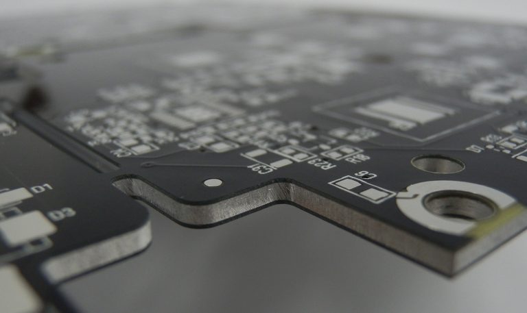
Once the circuit pattern is established, the next step is the application of the immersion gold finish.
This process, known as electroless nickel immersion gold (ENIG), involves the deposition of a thin layer of nickel followed by a layer of gold onto the exposed copper traces. The nickel layer acts as a barrier to prevent copper diffusion, while the gold layer provides excellent conductivity and resistance to oxidation. The immersion gold finish is particularly advantageous for high-frequency PCBs as it ensures a smooth, flat surface that is ideal for soldering and provides a stable contact surface for connectors.
After the application of the immersion gold finish, the PCB undergoes a series of inspections and tests to ensure its quality and performance.
These tests include electrical testing to verify the integrity of the circuit connections and impedance testing to ensure that the PCB meets the required specifications for high-frequency applications. Any defects or deviations from the design specifications are addressed before the PCB is approved for assembly.
Finally, the completed high-frequency PCB is ready for assembly, where components are mounted onto the board.
The use of immersion gold ensures that the solder joints are reliable and that the connections between the components and the PCB are robust. This is crucial for high-frequency applications, where even minor imperfections can lead to significant signal degradation.
In conclusion, the manufacturing process of high-frequency PCBs with immersion gold is a meticulous and highly technical procedure. It involves careful material selection, precise fabrication techniques, and rigorous testing to ensure that the final product meets the demanding requirements of high-frequency applications. The use of immersion gold not only enhances the performance of these PCBs but also ensures their reliability and longevity in critical applications.
Comparing Immersion Gold To Other Surface Finishes For High-Frequency PCBs
In the realm of high-frequency printed circuit boards (PCBs), selecting the appropriate surface finish is crucial to ensuring optimal performance and reliability. Among the various options available, immersion gold has emerged as a popular choice, particularly for high-frequency applications. To understand its advantages, it is essential to compare immersion gold with other prevalent surface finishes, such as hot air solder leveling (HASL), electroless nickel immersion gold (ENIG), and organic solderability preservatives (OSP).
Immersion gold, a subset of the ENIG process, involves depositing a thin layer of gold over a nickel barrier.
This finish is renowned for its excellent conductivity and corrosion resistance, which are critical for high-frequency PCBs. The smooth and flat surface provided by immersion gold ensures minimal signal loss and impedance discontinuities, which are vital for maintaining signal integrity at high frequencies. In contrast, HASL, which involves coating the PCB with molten solder, often results in an uneven surface. This irregularity can lead to signal distortion and increased insertion loss, making HASL less suitable for high-frequency applications.
Furthermore, immersion gold offers superior durability compared to OSP.
While OSP is a cost-effective and environmentally friendly option, it provides only a thin protective layer that can be easily compromised during handling and assembly. This vulnerability can lead to oxidation and degradation of the copper pads, adversely affecting the performance of high-frequency circuits. In contrast, the robust nickel-gold layer in immersion gold provides a more reliable barrier against environmental factors, ensuring long-term stability and performance.
Another critical aspect to consider is the compatibility of the surface finish with fine-pitch components.
As electronic devices continue to shrink in size, the demand for PCBs with fine-pitch components has increased. Immersion gold excels in this regard due to its ability to produce a uniform and flat surface, which is essential for achieving reliable solder joints with fine-pitch components. On the other hand, HASL’s uneven surface can pose challenges in achieving consistent soldering results, potentially leading to defects such as bridging or insufficient solder joints.
Moreover, the choice of surface finish can significantly impact the assembly process.
Immersion gold is known for its excellent solderability, which facilitates efficient and reliable assembly. The gold layer provides a highly solderable surface that reduces the risk of defects during the soldering process. In comparison, OSP, while offering good initial solderability, may require additional handling precautions to prevent oxidation before assembly, adding complexity to the manufacturing process.
Cost considerations also play a role in the selection of surface finishes.
While immersion gold is generally more expensive than HASL and OSP, its benefits in terms of performance, reliability, and ease of assembly often justify the additional cost, especially for high-frequency applications where signal integrity is paramount. The long-term reliability and reduced risk of defects can lead to cost savings in terms of reduced rework and improved product lifespan.
In conclusion, when comparing immersion gold to other surface finishes for high-frequency PCBs, it becomes evident that immersion gold offers distinct advantages in terms of signal integrity, durability, and compatibility with fine-pitch components. While it may come at a higher initial cost, the benefits it provides in ensuring reliable and high-performance PCBs make it a compelling choice for applications where maintaining signal integrity is critical. As technology continues to advance, the demand for high-frequency PCBs with superior performance will likely drive further adoption of immersion gold as a preferred surface finish.
Challenges And Solutions In Using Immersion Gold For High-Frequency PCBs
The use of immersion gold in high-frequency printed circuit boards (PCBs) presents a unique set of challenges and solutions that are critical for engineers and manufacturers to understand. As the demand for high-frequency applications continues to grow, driven by advancements in telecommunications, aerospace, and consumer electronics, the need for reliable and efficient PCB materials becomes increasingly important. Immersion gold, a popular surface finish for PCBs, offers several advantages, including excellent conductivity, corrosion resistance, and a smooth surface for soldering. However, its application in high-frequency PCBs is not without its difficulties.
One of the primary challenges associated with using immersion gold in high-frequency PCBs is the potential for signal loss.
High-frequency signals are particularly sensitive to the materials and finishes used in their construction. The presence of gold, while beneficial for its conductive properties, can introduce parasitic capacitance and inductance, which can degrade signal integrity. This is especially problematic in applications where maintaining signal fidelity is crucial, such as in RF and microwave circuits. To address this issue, careful consideration must be given to the thickness of the gold layer. A thinner gold layer can help minimize these parasitic effects, but it must be balanced against the need for durability and corrosion resistance.
Another challenge is the potential for increased production costs.
Immersion gold is more expensive than other surface finishes, such as HASL (Hot Air Solder Leveling) or OSP (Organic Solderability Preservatives). This cost is further compounded by the need for precise control over the deposition process to ensure uniformity and adherence to specifications. Manufacturers must weigh the benefits of using immersion gold against these increased costs, particularly in high-volume production scenarios. To mitigate these expenses, some manufacturers are exploring hybrid approaches, combining immersion gold with other, less costly finishes in areas where high-frequency performance is less critical.
Furthermore, the environmental impact of using gold in PCBs cannot be overlooked.
The extraction and processing of gold are resource-intensive and can have significant ecological consequences. As a result, there is a growing push within the industry to develop more sustainable practices and materials. Some companies are investing in research to find alternative finishes that offer similar performance characteristics without the environmental drawbacks. Additionally, recycling and reclaiming gold from used PCBs is becoming an increasingly viable option, helping to reduce the overall environmental footprint.
Despite these challenges, the use of immersion gold in high-frequency PCBs offers several compelling solutions.
Its excellent solderability and corrosion resistance make it an ideal choice for applications where reliability is paramount. Moreover, advancements in deposition technology are enabling more precise control over the gold layer, reducing the risk of signal degradation. By leveraging these technological improvements, manufacturers can optimize the performance of high-frequency PCBs while minimizing the associated drawbacks.
In conclusion, while the use of immersion gold in high-frequency PCBs presents certain challenges, these can be effectively managed through careful design considerations and technological advancements. By addressing issues such as signal loss, production costs, and environmental impact, manufacturers can harness the benefits of immersion gold to meet the demands of modern high-frequency applications. As the industry continues to evolve, ongoing research and innovation will undoubtedly lead to even more effective solutions, ensuring that immersion gold remains a valuable tool in the development of high-performance PCBs.