Immersion Silver PCB: A Comprehensive Guide to Surface Finish Technology
1. Introduction
Printed Circuit Boards (PCBs) are essential components in modern electronics, providing mechanical support and electrical connections for electronic components. One critical aspect of PCB manufacturing is the surface finish, which protects the copper traces from oxidation and ensures reliable solderability. Among the various surface finishes available, Immersion Silver (IAg) has gained significant popularity due to its excellent electrical performance, cost-effectiveness, and environmental benefits.
This article explores Immersion Silver PCB technology, covering its manufacturing process, advantages, disadvantages, applications, and comparisons with other surface finishes.
2. What is Immersion Silver PCB?
Immersion Silver is a metallic surface finish applied to PCBs through a chemical displacement process. A thin layer of silver (typically 0.1 to 0.3 microns) is deposited on the exposed copper traces, providing a flat, solderable surface. Unlike electroplated silver, immersion silver does not require an external electrical current, making it a simpler and more cost-effective solution.
Key Characteristics of Immersion Silver PCB:
- Thickness: 0.1–0.3 µm
- Shelf Life: 6–12 months (depending on storage conditions)
- Solderability: Excellent for lead-free soldering
- Surface Flatness: Ideal for fine-pitch components
- Environmental Impact: RoHS compliant, no harsh chemicals like ENIG (Electroless Nickel Immersion Gold)
3. Manufacturing Process of Immersion Silver PCB
The immersion silver process involves several key steps:
Step 1: Cleaning and Microetching
- The PCB undergoes cleaning to remove organic contaminants and oxides.
- A microetching step (using sodium persulfate or sulfuric acid-hydrogen peroxide) roughens the copper surface for better silver adhesion.
Step 2: Pre-Dip (Acid Treatment)
- The board is dipped in a mild acid solution to remove residual oxides and prepare the copper for silver deposition.
Step 3: Immersion Silver Deposition
- The PCB is immersed in a silver solution (typically containing silver nitrate and organic additives).
- A displacement reaction occurs where silver ions replace copper atoms on the surface:
[
Cu + 2Ag^+ → Cu^{2+} + 2Ag
] - The process is self-limiting, meaning the reaction stops once all exposed copper is coated.
Step 4: Post-Treatment and Drying
- A protective organic layer (often an anti-tarnish agent) is applied to prevent silver oxidation.
- The PCB is rinsed and dried to avoid moisture retention.
4. Advantages of Immersion Silver PCB
① Excellent Solderability
- Silver provides a highly solderable surface, making it suitable for lead-free (SAC305) soldering.
- Performs well in reflow and wave soldering processes.
② Superior Electrical Conductivity
- Silver has the highest electrical conductivity among metals, reducing signal loss in high-frequency and RF applications.
③ Flat Surface for Fine-Pitch Components
- Unlike HASL (Hot Air Solder Leveling), immersion silver provides a flat surface, essential for BGA, QFN, and fine-pitch ICs.
④ Cost-Effective Compared to ENIG
- Lower cost than ENIG (Electroless Nickel Immersion Gold) while maintaining good performance.
⑤ RoHS Compliance & Environmental Benefits
- Does not contain lead or harsh chemicals, making it environmentally friendly.
5. Disadvantages and Challenges
Despite its advantages, immersion silver has some limitations:
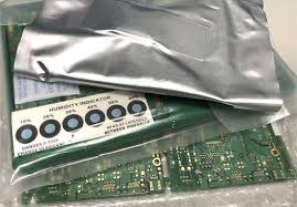
① Limited Shelf Life
- Silver can tarnish over time due to sulfur exposure (forming Ag₂S).
- Proper storage (anti-tarnish packaging) is required to extend shelf life.
② Risk of Silver Migration (Whiskers)
- Under high humidity, dendritic growth (silver whiskers) can cause short circuits.
- Mitigated by conformal coating or controlled storage conditions.
③ Not Suitable for Multiple Reflow Cycles
- Excessive thermal cycling can degrade the silver layer, unlike ENIG, which withstands multiple reflows.
6. Applications of Immersion Silver PCB
Immersion silver is widely used in:
- Consumer Electronics (Smartphones, Tablets, Laptops)
- Automotive Electronics (ECUs, Sensors)
- Telecommunications (5G, RF Modules)
- Medical Devices (Wearables, Diagnostic Equipment)
- Industrial Control Systems (High-Speed PCBs)
7. Comparison with Other PCB Surface Finishe
| Surface Finish | Thickness | Solderability | Cost | Shelf Life | Best For |
|---|---|---|---|---|---|
| Immersion Silver (IAg) | 0.1–0.3 µm | Excellent | Medium | 6–12 months | High-frequency, fine-pitch |
| ENIG (Ni/Au) | Ni: 3–5 µm, Au: 0.05–0.1 µm | Very Good | High | 12+ months | BGA, HDI, harsh environments |
| HASL (Lead-Free) | 1–25 µm | Good | Low | 12 months | Cost-sensitive, non-fine-pitch |
| OSP (Organic Solderability Preservative) | 0.2–0.5 µm | Fair | Low | 6 months | Simple boards, short-term use |
| Immersion Tin (ISn) | 0.8–1.2 µm | Good | Medium | 6–12 months | Press-fit connectors |
8. Future Trends in Immersion Silver Technology
- Improved Anti-Tarnish Coatings to extend shelf life.
- Hybrid Finishes (e.g., Silver + OSP) for enhanced durability.
- Adoption in High-Speed PCBs for 5G and IoT applications.
9. Conclusion
Immersion Silver PCB is a high-performance, cost-effective surface finish suitable for modern electronics requiring fine-pitch components and high-frequency signal integrity. While it has some challenges (tarnishing, whisker growth), proper handling and storage can mitigate these issues.
As the demand for lead-free, RoHS-compliant PCBs grows, immersion silver remains a strong alternative to ENIG and HASL, particularly in consumer electronics, automotive, and telecommunications.
By understanding its benefits, limitations, and best-use cases, engineers and manufacturers can make informed decisions when selecting PCB surface finishes.


