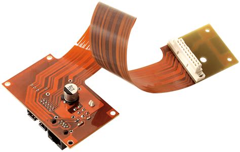
Impedance flex pcb
Understanding Impedance Control in Flexible PCBs
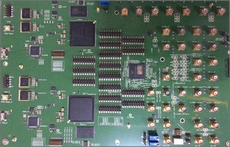
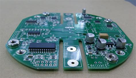
Impedance control in flexible printed circuit boards (PCBs) is a critical aspect of modern electronics design, particularly as devices become more compact and complex. Flexible PCBs, known for their ability to bend and conform to various shapes, are increasingly used in applications ranging from consumer electronics to medical devices. As these applications often involve high-speed signals, maintaining signal integrity through impedance control becomes paramount.
To understand impedance control in flexible PCBs, it is essential to first grasp the concept of impedance itself.
Impedance, in the context of PCBs, refers to the resistance a circuit offers to the flow of alternating current (AC). It is a combination of resistance, inductance, and capacitance, and is measured in ohms. In high-frequency applications, controlling impedance is crucial to ensure that signals are transmitted without distortion or loss. This is because any mismatch in impedance can lead to reflections, which degrade signal quality and can cause data errors.
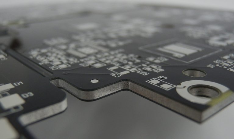
Flexible PCBs present unique challenges for impedance control due to their inherent material properties and structural characteristics.
Unlike rigid PCBs, flexible circuits are made from materials such as polyimide or polyester, which have different dielectric constants and loss tangents. These materials can affect the impedance of the circuit, necessitating careful design considerations. Moreover, the ability of flexible PCBs to bend and twist means that the physical dimensions of the traces can change, further complicating impedance control.
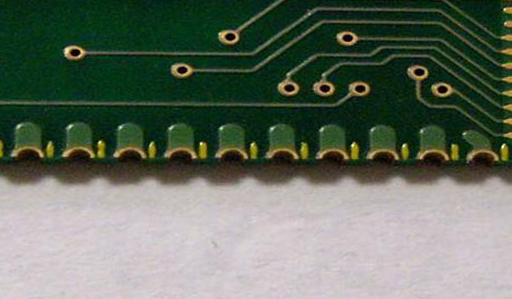
To achieve precise impedance control in flexible PCBs, designers must consider several factors.
One of the primary considerations is the trace width and spacing. The geometry of the traces directly influences the impedance, and any variations can lead to inconsistencies. Therefore, maintaining uniform trace dimensions is crucial. Additionally, the thickness of the dielectric material between the trace and the ground plane plays a significant role in determining impedance. By adjusting these parameters, designers can achieve the desired impedance levels.
Another important aspect is the choice of materials.
The dielectric constant of the substrate material affects the impedance, and selecting a material with a stable dielectric constant over the operating frequency range is vital. Furthermore, the use of advanced simulation tools allows designers to model and predict the impedance characteristics of flexible PCBs accurately. These tools enable the optimization of trace layouts and material selections before the actual fabrication process, reducing the risk of impedance mismatches.
Moreover, the manufacturing process itself can impact impedance control.
Variations in etching, lamination, and other fabrication steps can introduce discrepancies in trace dimensions and dielectric thickness. Therefore, working closely with experienced manufacturers who understand the nuances of flexible PCB production is essential to ensure that the designed impedance specifications are met.
In conclusion, impedance control in flexible PCBs is a complex but essential aspect of modern electronics design. As devices continue to shrink and operate at higher frequencies, maintaining signal integrity through precise impedance control becomes increasingly important. By understanding the interplay between materials, trace geometry, and manufacturing processes, designers can create flexible PCBs that meet the stringent requirements of today’s high-speed applications. Through careful planning and collaboration with skilled manufacturers, the challenges of impedance control in flexible PCBs can be effectively addressed, ensuring reliable and efficient electronic devices.
Design Techniques for Impedance Matching in Flex PCBs
Impedance matching in flexible printed circuit boards (flex PCBs) is a critical design consideration that ensures signal integrity and optimal performance in electronic devices. As electronic devices become increasingly compact and complex, the demand for flex PCBs has surged due to their ability to bend and conform to various shapes. However, this flexibility introduces unique challenges in maintaining consistent impedance, which is crucial for high-frequency signal transmission. To address these challenges, designers employ several techniques to achieve impedance matching in flex PCBs.
One fundamental technique involves the careful selection of materials.
The dielectric constant of the substrate material significantly influences the impedance of the circuit. By choosing materials with stable dielectric properties, designers can maintain consistent impedance across the flex PCB. Additionally, the thickness of the dielectric layer plays a vital role. Thinner dielectric layers can lead to lower impedance, while thicker layers can increase it. Therefore, precise control over material thickness is essential to achieve the desired impedance levels.
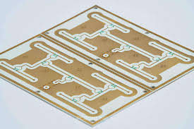
Moreover, the geometry of the conductive traces is another critical factor in impedance matching.
The width and spacing of the traces, as well as their proximity to the ground plane, directly affect the impedance. Designers often use simulation tools to model and optimize trace geometries, ensuring that they meet the required impedance specifications. By adjusting these parameters, it is possible to fine-tune the impedance and minimize signal reflections, which can degrade performance.
Transitioning to another important aspect, the use of controlled impedance traces is a common practice in flex PCB design.
Controlled impedance traces are designed to have a specific impedance value, typically 50 or 75 ohms, which matches the impedance of the connected components and transmission lines. This matching minimizes signal reflections and ensures efficient power transfer. To achieve controlled impedance, designers must consider the trace width, thickness, and the dielectric constant of the substrate, as well as the distance between the trace and the reference plane.
Furthermore, the implementation of ground planes and reference layers is crucial in maintaining consistent impedance.
Ground planes provide a return path for signals and help reduce electromagnetic interference (EMI). By placing a ground plane close to the signal traces, designers can create a controlled impedance environment. This proximity helps stabilize the impedance and reduces the risk of signal distortion. Additionally, using multiple reference layers can further enhance signal integrity by providing additional paths for return currents.
In addition to these techniques, the use of advanced simulation and modeling tools is indispensable in modern flex PCB design.
These tools allow designers to predict and analyze the impedance characteristics of their designs before fabrication. By simulating different scenarios and configurations, designers can identify potential issues and make necessary adjustments to ensure impedance matching. This proactive approach not only saves time and resources but also enhances the reliability and performance of the final product.
In conclusion, achieving impedance matching in flex PCBs requires a comprehensive understanding of material properties, trace geometries, and the strategic use of ground planes and reference layers. By employing these design techniques and leveraging advanced simulation tools, designers can overcome the challenges posed by the flexible nature of these circuits. As technology continues to evolve, the importance of impedance matching in flex PCBs will only grow, underscoring the need for meticulous design practices to ensure optimal performance in increasingly sophisticated electronic devices.
Challenges and Solutions in Impedance Testing for Flexible PCBs
Impedance testing for flexible printed circuit boards (PCBs) presents a unique set of challenges that require innovative solutions to ensure optimal performance and reliability. As the demand for smaller, lighter, and more versatile electronic devices continues to grow, flexible PCBs have become increasingly popular due to their ability to bend and conform to various shapes. However, this flexibility introduces complexities in impedance testing that are not typically encountered with rigid PCBs.
One of the primary challenges in impedance testing for flexible PCBs is the variability in material properties.
Flexible PCBs are often made from materials such as polyimide or polyester, which can exhibit different dielectric constants and loss tangents compared to the materials used in rigid PCBs. This variability can lead to inconsistencies in impedance measurements, making it difficult to ensure that the PCB will perform as expected in its intended application. To address this issue, it is essential to carefully select materials with well-characterized electrical properties and to use precise manufacturing processes that minimize variations.
Another challenge is the impact of mechanical stress on impedance.
Flexible PCBs are designed to bend and flex, but this mechanical movement can alter the electrical characteristics of the circuit, potentially affecting impedance. For instance, repeated bending can cause micro-cracks or delamination in the conductive traces, leading to changes in impedance. To mitigate these effects, designers can incorporate stress-relief features into the PCB layout, such as curved traces and strategically placed vias, which help distribute mechanical stress more evenly across the board.
Moreover, the testing environment itself can pose challenges.
Flexible PCBs are often used in applications where they are exposed to harsh conditions, such as extreme temperatures or humidity. These environmental factors can influence impedance by affecting the material properties or causing physical deformation of the PCB. To ensure accurate impedance testing, it is crucial to simulate the operating conditions during the testing phase. This can be achieved by using environmental chambers that replicate the temperature and humidity levels the PCB will encounter in real-world applications.
In addition to these challenges, the miniaturization of electronic components further complicates impedance testing.
As devices become smaller, the traces and spaces on flexible PCBs must also shrink, increasing the risk of impedance mismatches. Advanced testing equipment with high precision and sensitivity is required to accurately measure impedance in these miniature circuits. Furthermore, employing simulation tools during the design phase can help predict potential impedance issues and allow for adjustments before the manufacturing process begins.
Despite these challenges, several solutions have been developed to improve impedance testing for flexible PCBs.
One such solution is the use of time-domain reflectometry (TDR), a technique that allows for precise measurement of impedance along the length of a trace. TDR can identify discontinuities and impedance mismatches, providing valuable insights into the PCB’s performance. Additionally, advancements in computer-aided design (CAD) software have enabled more accurate modeling of flexible PCBs, allowing designers to optimize impedance characteristics before physical prototypes are produced.
In conclusion, while impedance testing for flexible PCBs presents several challenges, a combination of careful material selection, innovative design strategies, and advanced testing techniques can effectively address these issues. By understanding and overcoming these challenges, manufacturers can ensure that flexible PCBs meet the stringent performance and reliability requirements of modern electronic devices. As technology continues to evolve, ongoing research and development will undoubtedly lead to even more sophisticated solutions for impedance testing in flexible PCBs.
The Role of Impedance in High-Frequency Flex PCB Applications
In the realm of modern electronics, the demand for compact, efficient, and high-performance devices has led to the increasing use of flexible printed circuit boards (PCBs). Among the various considerations in designing these advanced circuits, impedance control emerges as a critical factor, particularly in high-frequency applications. Impedance, in the context of PCBs, refers to the resistance encountered by an alternating current as it travels through the circuit. This resistance is not merely a function of the conductive material but also depends on the frequency of the signal, the geometry of the traces, and the dielectric properties of the materials used.
As electronic devices continue to shrink in size while expanding in functionality, the need for high-frequency signals to travel through flexible PCBs without distortion becomes paramount.
Impedance control ensures that these signals maintain their integrity, which is crucial for the performance of high-speed data transmission. Inflexible PCBs, the challenge of impedance control is compounded by the inherent flexibility of the substrate, which can lead to variations in trace geometry and dielectric properties. Therefore, precise design and manufacturing processes are essential to maintain consistent impedance across the board.
To achieve the desired impedance in flex PCBs, designers must carefully consider several factors.
The width and thickness of the conductive traces, the spacing between them, and the properties of the dielectric material all play significant roles. Additionally, the stack-up configuration of the PCB layers can influence impedance. By adjusting these parameters, designers can tailor the impedance to match the requirements of specific high-frequency applications. This meticulous design process often involves the use of advanced simulation tools to predict the impedance characteristics of the PCB before it is manufactured.
Moreover, the choice of materials is crucial in impedance-controlled flex PCBs.
The dielectric constant and loss tangent of the substrate material can significantly affect the impedance. Materials with low dielectric constants and loss tangents are preferred for high-frequency applications as they minimize signal loss and distortion. Polyimide is a common choice for flex PCBs due to its excellent electrical properties and flexibility. However, as the demand for higher frequencies and faster data rates increases, new materials with even better performance characteristics are being developed.
In addition to design and material considerations, the manufacturing process also plays a vital role in achieving the desired impedance.
Precision in etching the conductive traces and maintaining consistent layer thicknesses is essential. Any deviation from the intended design can lead to impedance mismatches, resulting in signal reflections and loss. Therefore, manufacturers must employ stringent quality control measures to ensure that the final product meets the specified impedance requirements.
Furthermore, testing and validation are integral to the development of impedance-controlled flex PCBs.
Once manufactured, these PCBs undergo rigorous testing to verify their impedance characteristics. Techniques such as time-domain reflectometry (TDR) and vector network analysis are commonly used to measure impedance and identify any discrepancies from the design specifications. This testing ensures that the flex PCBs will perform reliably in their intended high-frequency applications.
In conclusion, impedance control is a fundamental aspect of designing and manufacturing flex PCBs for high-frequency applications. By carefully considering design parameters, material properties, and manufacturing processes, engineers can create flexible circuits that meet the demanding requirements of modern electronic devices. As technology continues to advance, the role of impedance in flex PCBs will remain a critical factor in enabling the next generation of high-performance electronics.