Implementing ESD Protection in PCB Design: Strategies and Best Practices
Introduction
Electrostatic discharge (ESD) is a sudden flow of electricity between two electrically charged objects, often caused by contact, electrical shorting, or dielectric breakdown. In printed circuit board (PCB) design, ESD can cause catastrophic failures, latent defects, or performance degradation in electronic components. Proper ESD protection is crucial to ensure reliability, especially in high-speed and high-frequency applications.
This article explores key strategies for implementing ESD protection in PCB design, including layout techniques, component selection, grounding methods, and testing considerations.
1. Understanding ESD and Its Impact on PCBs
1.1 Sources of ESD
ESD can originate from:
- Human handling (e.g., touching components without proper grounding)
- Triboelectric charging (friction between materials)
- Inductive coupling from nearby electrostatic fields
1.2 Effects of ESD on PCBs
- Immediate damage: Burned traces, fried ICs, or blown capacitors.
- Latent damage: Weakened components that fail later under normal operation.
- Signal integrity issues: Noise coupling, false triggering, or data corruption.
2. Key Strategies for ESD Protection in PCB Design
2.1 Proper Grounding Techniques
A solid grounding strategy is the first line of defense against ESD.
2.1.1 Single-Point vs. Multi-Point Grounding
- Single-point grounding: Best for low-frequency designs to avoid ground loops.
- Multi-point grounding: Preferred for high-speed designs to minimize impedance.
2.1.2 Ground Plane Design
- Use a continuous ground plane to provide a low-impedance return path.
- Avoid splits in the ground plane under sensitive components.
- Implement a “quiet ground” for analog and RF sections to prevent noise coupling.
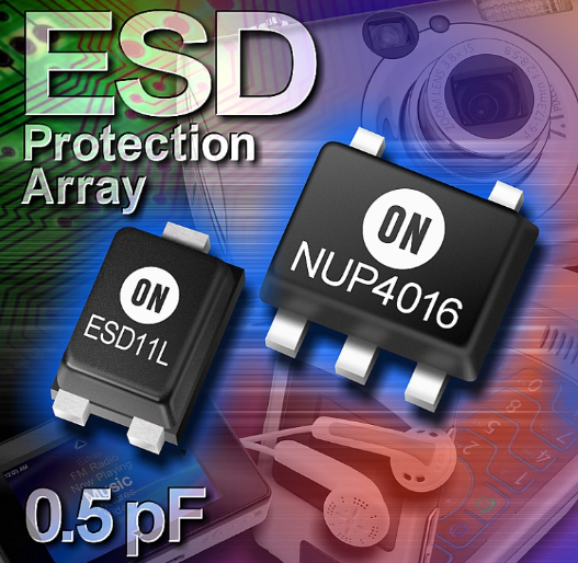
2.2 ESD Protection Components
2.2.1 TVS Diodes (Transient Voltage Suppressors)
- Fast-acting diodes that clamp ESD pulses to a safe voltage level.
- Place TVS diodes near connectors and I/O ports.
- Select diodes with appropriate breakdown voltage (e.g., 5V for USB, 12V for RS-232).
2.2.2 Ferrite Beads and EMI Filters
- Used to suppress high-frequency noise from ESD events.
- Effective for filtering power and signal lines.
2.2.3 Spark Gaps and ESD Suppressors
- Spark gaps provide a physical discharge path but require careful spacing.
- Polymer-based ESD suppressors can absorb and dissipate ESD energy.
2.3 PCB Layout Techniques for ESD Mitigation
2.3.1 Trace Routing Best Practices
- Keep high-speed traces away from board edges.
- Minimize loop areas to reduce inductive coupling.
- Use 90-degree rounded corners instead of sharp angles to avoid charge accumulation.
2.3.2 Component Placement
- Place ESD-sensitive components (e.g., microcontrollers, sensors) away from high-risk zones (connectors, buttons).
- Implement guard rings around critical components to divert ESD currents.
2.3.3 Shielding and Enclosure Design
- Use metal shielding cans for RF and high-speed circuits.
- Ensure proper enclosure grounding to prevent charge buildup.
2.4 Isolation and Signal Integrity
2.4.1 Optocouplers and Isolation Transformers
- Useful for isolating sensitive circuits from high-voltage sections.
2.4.2 Differential Signaling
- Reduces susceptibility to ESD-induced noise (e.g., USB, Ethernet).
3. Testing and Validation
3.1 ESD Testing Standards (IEC 61000-4-2)
- Contact discharge: Direct application of ESD to conductive surfaces.
- Air discharge: Simulates real-world ESD events near the PCB.
3.2 Common ESD Testing Methods
- Human Body Model (HBM): Simulates ESD from human touch.
- Charged Device Model (CDM): Simulates ESD from charged components.
3.3 Post-Test Analysis
- Inspect for physical damage (burnt traces, cracked ICs).
- Verify signal integrity with oscilloscope or spectrum analyzer.
4. Industry Best Practices
- Use ESD-safe materials (e.g., antistatic coatings, conductive foam).
- Implement ESD protection early in the design phase.
- Train personnel on proper ESD handling (wrist straps, grounded workstations).
Conclusion
ESD protection in PCB design requires a multi-layered approach, combining proper grounding, strategic component placement, and effective shielding. By following industry best practices and adhering to ESD testing standards, designers can significantly improve the reliability and longevity of electronic devices.
Future advancements in materials science and semiconductor technology may offer even stronger ESD protection solutions, but the fundamentals of good PCB design will remain essential.


