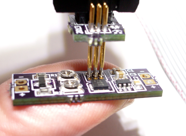
Improvement method of hole/permeation problem when using PCB dry
Dry film masking holes appear broken
Many customers believe that after the occurrence of broken holes, the film temperature and pressure should be increased to enhance the bonding force. In fact, this view is incorrect. Because the temperature and pressure are too high, the solvent of the resist is excessively volatilized and dried. The film becomes brittle and thin, and it is easy to be broken through the hole during development. We always have to maintain the toughness of the dry film. Therefore, after the hole is broken, we can improve from the following points:
1, reduce film temperature and pressure
2, improve the drilling cloak
3, increase exposure energy
4, reduce the development pressure
5, the parking time after filming can not be too long, so as not to cause the semi-fluid film at the corner to spread and become thin under the pressure
6, the dry film should not be too tight during the filming process
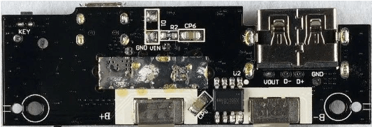
Second, the appearance of plating during dry film plating
The reason why the plating is performed indicates that the dry film and the copper clad plate are not firmly bonded, so that the plating solution is deep, and the coating of the “negative phase” is thickened. The plating of most PCB manufacturers is caused by the following points:
1, the exposure energy is high or low
Under ultraviolet light irradiation, the photoinitiator that absorbs the light energy decomposes into a radical to initiate a photopolymerization reaction to form a bulk molecule which is insoluble in a solution of a dilute alkali. When the exposure is insufficient, due to incomplete polymerization, during the development process, the film swells and becomes soft, resulting in unclear lines or even falling off of the film, resulting in poor bonding of the film to copper; if overexposed, it may cause development difficulties, and also during the electroplating process. The warp peeling occurs in the middle to form a plating. So it is important to control the exposure energy.
2, the film temperature is high or low
If the film temperature is too low, the surface of the dry film and the copper clad laminate may be poorly bonded due to insufficient softening and proper flow of the resist film; if the temperature is too high, the solvent and other volatiles in the resist may be caused. The rapid evaporation of the substance generates bubbles, and the dry film becomes brittle, forming a warp peeling during electroplating, causing plating.
3, the film pressure is high or low
When the film pressure is too low, the film surface may be uneven or a gap may be formed between the dry film and the copper plate to meet the bonding force requirement; if the film pressure is too high, the solvent and volatile components of the resist layer are excessively volatilized, resulting in excessive evaporation. The dry film becomes brittle and will peel off after electroplating.
About the relationship between PI and FPC boards
PI refers to a polyimide resin material, which is now widely used in various fields and is a very good material. Some people call PI a symbolic material that promotes the reform of electronic products. . We mainly explain the location and role of FPC and PI.
PI is a material with very good high temperature resistance and will be used in aerospace technology. PI has two main locations in the board.
1. As a circuit board substrate
This is the material that most boards are used in. The board mainly plays a role of reinforcement and thickening, mainly because the copper foil of the board is very thin, not enough to support the glue and the cover film separately. In this position of use, the PI is mainly a layer having a plurality of layers of PI for lamination, and the PI of the single layer is also very thin.
PI is not the only material used as a substrate, and there are also like PET, FR4, ET, etc., but because the soft board is affected by the material shrinkage during production, it is produced for the production yield and efficiency. Most of the FPC flexible circuit boards are made of PI as the insulating material, unless the customer requests other materials.
2. As a cover film
The single-layer PI is very thin, and PI has a variety of properties, not only high temperature resistance, but also excellent in wear resistance and insulation. Therefore, in the place where the gold finger of the circuit board is used, the role of the PI as a protective film is often used, mainly because the gold finger needs a very connector to perform the embedding time, and the use of the ordinary cover film is long and the gold finger damage is easy.