Improving PCB Warpage: Causes, Measurement, and Effective Solutions
Introduction to PCB Warpage
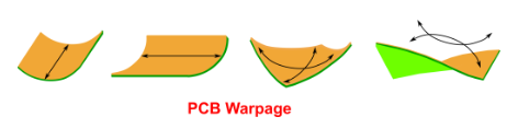
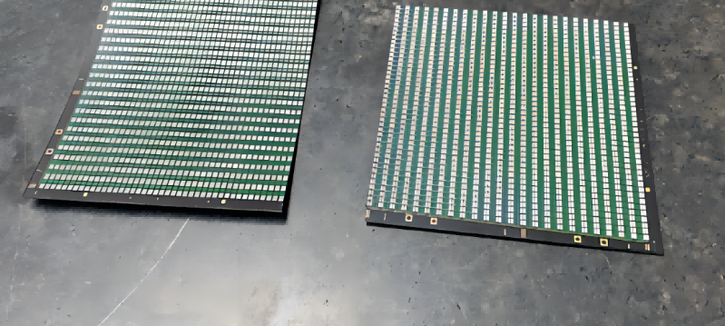
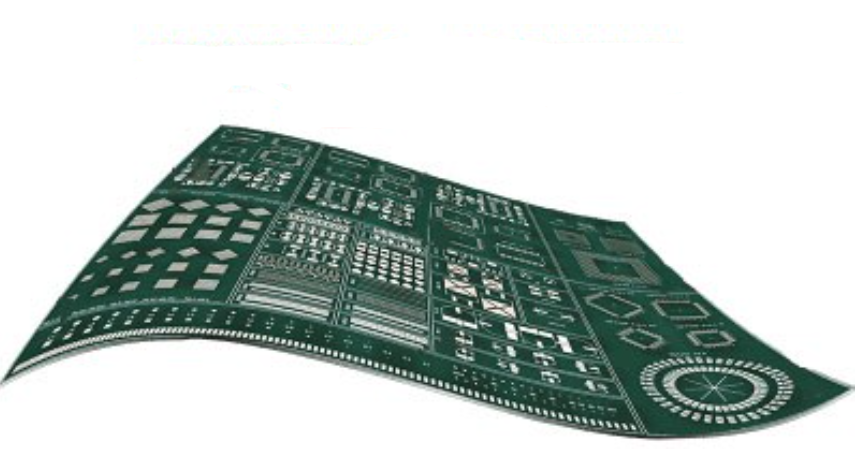
Printed Circuit Board (PCB) warpage, also known as board deformation or bending, is a common issue in the electronics manufacturing industry that can significantly impact product quality and reliability. PCB warpage refers to the undesired bending or twisting of a circuit board from its ideal flat plane, which can occur during various stages of manufacturing, assembly, or even in end-use applications.
The importance of addressing PCB warpage cannot be overstated in modern electronics manufacturing. As electronic devices continue to shrink in size while increasing in complexity, even minor board deformations can lead to serious problems:
- Component placement issues in surface mount technology (SMT) assembly
- Poor solder joint quality leading to open circuits or weak connections
- Mechanical stress on components and interconnects
- Assembly process failures in automated production lines
- Reduced product reliability and shortened lifespan
With the industry trend toward thinner boards, higher layer counts, and larger panel sizes, the challenge of controlling PCB warpage has become increasingly critical. This article will examine the root causes of PCB deformation, methods for measuring warpage, and comprehensive strategies for prevention and correction throughout the manufacturing and assembly processes.
Causes of PCB Warpage
Understanding the fundamental causes of PCB warpage is essential for developing effective prevention strategies. The deformation of circuit boards typically results from a combination of material properties, design factors, and manufacturing processes.
Material-Related Causes
- CTE Mismatch: The coefficient of thermal expansion (CTE) differences between the various materials in a PCB stackup is the primary cause of warpage. Copper, prepreg, and core materials expand at different rates when heated during manufacturing processes like lamination and soldering.
- Asymmetrical Layer Stackup: Uneven distribution of copper layers or unbalanced material placement across the board’s central plane creates inherent stresses that manifest as warpage.
- Material Quality Variations: Inconsistencies in prepreg resin content, glass cloth properties, or copper foil characteristics can lead to unpredictable warpage behavior.
Design-Related Causes
- Uneven Copper Distribution: Large copper areas on one side of the board without balancing copper on the opposite side create tension imbalances.
- High-Density Interconnects (HDI) Designs: Microvias and complex routing patterns can introduce localized stresses that contribute to overall board deformation.
- Panelization Issues: Poorly designed panel layouts with improper routing or breakout tabs can exacerbate warpage tendencies.
Manufacturing Process Causes
- Lamination Process: Improper lamination parameters (temperature, pressure, time) can lead to incomplete curing or excessive resin flow, causing residual stresses.
- Thermal Cycling: Repeated exposure to high temperatures during soldering, rework, or conformal coating processes can accumulate stress in the board structure.
- Mechanical Stress: Handling, depaneling, or improper storage conditions can induce physical deformation in otherwise flat boards.
- Moisture Absorption: PCBs exposed to humid environments can warp due to differential swelling of hygroscopic materials in the stackup.
Measuring and Evaluating PCB Warpage
Accurate measurement and quantification of PCB warpage are essential for process control and quality assurance. Several methods are commonly employed in the industry:
1. Warpage Gauge Measurement
The most traditional method uses a warpage gauge that physically measures the deviation from flatness at specified points on the board. This contact method provides direct measurements but is limited in resolution and throughput.
2. Shadow Moiré Technique
A non-contact optical method that projects a grating pattern onto the PCB surface and analyzes the distorted reflection to calculate warpage. This technique offers:
- High resolution (down to 10 microns)
- Full-field measurement across the entire board
- Capability for dynamic measurement during thermal cycling
3. Laser Scanning
Advanced laser displacement sensors can scan the PCB surface to create a detailed 3D map of surface topography, providing comprehensive warpage data with micron-level accuracy.
4. IPC Standards for Warpage Evaluation
The IPC-6012 and IPC-TM-650 standards define acceptable warpage limits:
- For SMT assemblies: typically ≤ 0.75% of board diagonal length
- For BGA packages: often stricter requirements of ≤ 0.50%
Measurement should be performed at room temperature (20-25°C) after proper conditioning, as warpage can vary significantly with temperature changes.
Strategies for Preventing PCB Warpage
Implementing proactive measures during design and manufacturing can significantly reduce the occurrence of PCB warpage:
Design Optimization Techniques
- Balanced Stackup Design:
- Maintain symmetry about the central plane
- Equal number of copper layers above and below center
- Similar copper density distribution on mirrored layers
- Copper Balancing:
- Add dummy copper fills in sparse areas
- Use hatched copper pours instead of solid when possible
- Balance power/ground plane coverage
- Material Selection:
- Choose materials with matched CTE characteristics
- Consider high-Tg materials for lead-free processes
- Evaluate low-loss materials for RF applications
- Panel Design Considerations:
- Optimize panel utilization while allowing for proper routing
- Include adequate breakaway tabs and mouse bites
- Consider scoring vs. routing for depaneling
Manufacturing Process Controls
- Lamination Process Optimization:
- Precisely control temperature ramp rates and dwell times
- Apply appropriate pressure profiles
- Implement proper cooling cycles
- Curing Process Management:
- Ensure complete resin cure without overexposure
- Monitor prepreg resin flow characteristics
- Verify glass transition temperatures (Tg)
- Moisture Control:
- Store PCBs in controlled humidity environments
- Implement pre-baking before high-temperature processes
- Use desiccant packs for moisture-sensitive boards
- Thermal Stress Reduction:
- Optimize reflow profiles to minimize thermal shock
- Implement graduated cooling after soldering
- Consider thermal cycling stabilization for critical boards
Correcting PCB Warpage Issues
When warpage occurs, several techniques can be employed to salvage affected boards:
1. Thermal Straightening
Controlled heating and weighting of warped boards can help relax internal stresses:
- Typically performed at temperatures near but below Tg
- Requires specialized flattening fixtures
- Must be followed by gradual cooling
2. Mechanical Flattening
For mild warpage, mechanical pressure can be applied:
- Often combined with thermal treatment
- Requires careful control to avoid damaging circuits
- Limited effectiveness for severe warpage
3. Process Adjustments
For consistent warpage patterns in production:
- Modify lamination parameters
- Adjust copper distribution in subsequent designs
- Change material specifications
4. Stress Relief Techniques
- Controlled vibration treatment
- Thermal cycling under constraint
- Humidity conditioning
Advanced Solutions for Challenging Applications
For particularly demanding applications or severe warpage issues, advanced solutions may be necessary:
1. Specialized PCB Materials
- Low-CTE laminates (e.g., polyimide, ceramic-filled)
- Metal-core substrates for improved thermal stability
- Composite materials with tailored expansion properties
2. Structural Reinforcement
- Strategic use of stiffeners in vulnerable areas
- Edge reinforcement techniques
- Selective thickening of critical sections
3. Process Innovations
- Sequential lamination for complex multilayer boards
- Low-stress via formation techniques
- Advanced curing monitoring systems
4. Predictive Modeling
- Finite element analysis (FEA) for warpage prediction
- Computational modeling of thermal-mechanical behavior
- Virtual prototyping to evaluate design alternatives
Conclusion
PCB warpage remains a significant challenge in electronics manufacturing, but through comprehensive understanding of its causes, precise measurement techniques, and implementation of robust prevention and correction strategies, manufacturers can achieve substantial improvements in board flatness. The key to success lies in:
- Holistic Approach: Addressing warpage requires attention to design, materials, and processes simultaneously
- Early Prevention: Implementing warpage-reduction strategies early in the design phase is most effective
- Process Control: Tight control of manufacturing parameters prevents many warpage issues
- Continuous Monitoring: Regular warpage measurement and analysis enables quick corrective action
As PCB technology continues to advance with thinner substrates, higher densities, and more complex architectures, the industry must develop corresponding advancements in warpage control methodologies. Future directions may include:
- Smart materials with self-correcting properties
- Real-time warpage monitoring during manufacturing
- AI-driven design optimization for minimal stress
- Nano-engineered composites with exceptional dimensional stability
By adopting the strategies outlined in this article and remaining vigilant about new developments in materials and processes, electronics manufacturers can significantly reduce PCB warpage-related defects, improve product quality, and enhance manufacturing yields in an increasingly competitive marketplace.