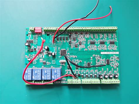
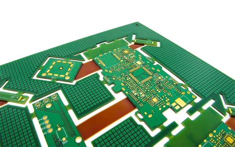
Ims pcb assembly
Understanding the Benefits of IMS PCB Assembly in Modern Electronics
In the rapidly evolving landscape of modern electronics, the demand for efficient, reliable, and high-performance components is ever-increasing.
One of the pivotal advancements in this domain is the development and implementation of Insulated Metal Substrate (IMS) Printed Circuit Board (PCB) assembly.
This technology has garnered significant attention due to its unique properties and the myriad benefits it offers to electronic devices. Understanding these advantages is crucial for manufacturers and designers aiming to optimize their products for better performance and durability.
To begin with, IMS PCB assembly is renowned for its exceptional thermal management capabilities.
Unlike traditional PCBs, which often struggle with heat dissipation, IMS PCBs are designed with a metal substrate that efficiently conducts heat away from critical components. This is particularly beneficial in high-power applications where excessive heat can lead to component failure or reduced lifespan. By effectively managing thermal output, IMS PCBs enhance the reliability and longevity of electronic devices, making them an ideal choice for applications such as LED lighting, power converters, and automotive electronics.
Moreover, the structural integrity of IMS PCBs is another compelling advantage.
The metal substrate not only aids in heat dissipation but also provides a robust foundation that enhances the mechanical stability of the board. This is especially important in environments subject to mechanical stress or vibration, where traditional PCBs might falter. The enhanced durability of IMS PCBs ensures that they can withstand harsh conditions without compromising performance, thus broadening their applicability across various industries.
In addition to thermal and mechanical benefits, IMS PCB assembly also contributes to improved electrical performance.
The design of IMS PCBs allows for shorter electrical paths, which reduces inductance and resistance. This results in more efficient power distribution and minimizes the potential for signal interference, which is crucial in high-frequency applications. Consequently, devices utilizing IMS PCBs can achieve superior performance metrics, which is a significant advantage in competitive markets where efficiency and speed are paramount.
Furthermore, the versatility of IMS PCB assembly cannot be overstated.
These boards can be customized to meet specific design requirements, offering flexibility in terms of size, shape, and layer configuration. This adaptability makes IMS PCBs suitable for a wide range of applications, from consumer electronics to industrial machinery. As technology continues to advance, the ability to tailor PCBs to meet precise specifications becomes increasingly valuable, allowing manufacturers to innovate and push the boundaries of what is possible.
While the benefits of IMS PCB assembly are clear, it is also important to consider the cost implications.
Initially, the production of IMS PCBs may be more expensive than traditional alternatives due to the materials and processes involved. However, the long-term savings achieved through enhanced performance, reduced failure rates, and extended product lifespans often outweigh the initial investment. As such, many companies view IMS PCB assembly as a strategic investment that can lead to significant competitive advantages.
In conclusion, IMS PCB assembly represents a significant advancement in the field of electronics, offering unparalleled benefits in terms of thermal management, structural integrity, electrical performance, and versatility. As the demand for high-performance electronic devices continues to grow, the adoption of IMS PCBs is likely to become increasingly prevalent. By understanding and leveraging the advantages of this technology, manufacturers can enhance the quality and reliability of their products, ultimately driving innovation and success in the modern electronics industry.
Key Challenges and Solutions in IMS PCB Assembly Processes
In the realm of electronics manufacturing, Insulated Metal Substrate (IMS) printed circuit boards (PCBs) have emerged as a pivotal component, particularly in applications requiring efficient heat dissipation. However, the assembly of IMS PCBs presents unique challenges that necessitate specialized solutions to ensure optimal performance and reliability. Understanding these challenges and their corresponding solutions is crucial for manufacturers aiming to leverage the benefits of IMS technology.
One of the primary challenges in IMS PCB assembly is thermal management.
IMS PCBs are often used in high-power applications where heat dissipation is critical. The metal substrate, typically aluminum or copper, provides a path for heat to be conducted away from heat-generating components. However, the assembly process must ensure that thermal interfaces are optimized to prevent hotspots and ensure uniform heat distribution. To address this, manufacturers often employ thermal interface materials (TIMs) that enhance thermal conductivity between components and the metal substrate. Additionally, precise control of solder reflow profiles is essential to prevent thermal stress and ensure reliable solder joints.
Another significant challenge is the mechanical stability of IMS PCBs.
The metal substrate, while excellent for thermal management, can introduce mechanical stresses during the assembly process. These stresses can lead to warping or deformation, particularly during soldering when the board is subjected to high temperatures. To mitigate this, manufacturers must carefully design the PCB layout to balance thermal and mechanical properties. This often involves strategic placement of vias and components to distribute stress evenly across the board. Furthermore, using advanced simulation tools during the design phase can help predict and alleviate potential mechanical issues.
Electrical isolation is also a critical concern in IMS PCB assembly.
The insulating layer between the metal substrate and the conductive copper traces must be robust enough to prevent electrical shorts while maintaining thermal conductivity. This requires precise control over the thickness and uniformity of the insulating layer during the manufacturing process. Advanced fabrication techniques, such as laser drilling and precision etching, are often employed to achieve the necessary tolerances and ensure reliable electrical isolation.
Moreover, the choice of materials plays a crucial role in overcoming the challenges associated with IMS PCB assembly.
Selecting the appropriate metal substrate, insulating material, and copper thickness can significantly impact the board’s thermal and electrical performance. Manufacturers must consider factors such as thermal conductivity, dielectric strength, and cost when choosing materials. Collaborating with material suppliers to develop customized solutions can also provide a competitive edge in meeting specific application requirements.
In addition to these technical challenges, the assembly of IMS PCBs must also address issues related to process scalability and cost-effectiveness.
As demand for IMS technology grows, manufacturers must develop efficient production processes that can be scaled to meet increasing volumes without compromising quality. This often involves investing in automated assembly equipment and implementing rigorous quality control measures to ensure consistency and reliability.
In conclusion, while IMS PCB assembly presents several challenges, a combination of advanced materials, precise manufacturing techniques, and strategic design considerations can effectively address these issues. By understanding and overcoming these challenges, manufacturers can fully exploit the advantages of IMS technology, delivering high-performance solutions for a wide range of applications. As the industry continues to evolve, ongoing research and innovation will undoubtedly lead to further advancements in IMS PCB assembly processes, paving the way for even more efficient and reliable electronic devices.

Innovations in IMS PCB Assembly: Trends to Watch in 2024
Innovations in IMS PCB assembly are poised to significantly impact the electronics manufacturing industry in 2024. As technology continues to advance, the demand for more efficient and reliable printed circuit boards (PCBs) has never been greater. IMS, or Insulated Metal Substrate, PCBs are particularly noteworthy due to their superior thermal management capabilities, making them ideal for high-power applications. As we look towards the future, several trends are emerging that promise to shape the landscape of IMS PCB assembly.
One of the most significant trends is the increasing integration of automation and artificial intelligence in the assembly process.
Automation has long been a staple in manufacturing, but recent advancements in AI are enabling even greater precision and efficiency. By utilizing machine learning algorithms, manufacturers can optimize the placement of components on IMS PCBs, reducing errors and improving overall production speed. This not only enhances the quality of the final product but also reduces costs, making IMS PCBs more accessible to a wider range of industries.
In addition to automation, the materials used in IMS PCB assembly are also evolving.
Traditionally, these PCBs have relied on aluminum as the primary substrate material due to its excellent thermal conductivity. However, new materials such as copper and advanced composites are being explored to further enhance performance. Copper, for instance, offers even better thermal management properties, which is crucial for applications that generate significant heat, such as LED lighting and power electronics. As these materials become more cost-effective, their adoption is expected to increase, leading to more efficient and durable IMS PCBs.
Moreover, the miniaturization of electronic components continues to drive innovation in IMS PCB assembly.
As devices become smaller and more powerful, the need for compact and efficient PCBs grows. This trend is pushing manufacturers to develop new techniques for assembling IMS PCBs that can accommodate smaller components without compromising performance. Techniques such as laser direct structuring and advanced soldering methods are being refined to meet these demands, ensuring that IMS PCBs remain at the forefront of technological advancement.
Sustainability is another critical factor influencing the future of IMS PCB assembly.
As environmental concerns become more pressing, manufacturers are seeking ways to reduce the ecological impact of their products. This includes using eco-friendly materials and processes that minimize waste and energy consumption. For instance, some companies are exploring the use of biodegradable substrates and lead-free soldering techniques to create more sustainable IMS PCBs. These efforts not only align with global sustainability goals but also appeal to environmentally conscious consumers and businesses.
Furthermore, the rise of the Internet of Things (IoT) is creating new opportunities for IMS PCB assembly.
As more devices become interconnected, the demand for PCBs that can handle increased data processing and communication capabilities is growing. IMS PCBs, with their excellent thermal management and reliability, are well-suited to meet these needs. Manufacturers are therefore focusing on developing IMS PCBs that can support the unique requirements of IoT applications, such as enhanced connectivity and energy efficiency.
In conclusion, the future of IMS PCB assembly is bright, with numerous innovations on the horizon. From automation and new materials to miniaturization and sustainability, these trends are set to redefine the industry in 2024 and beyond. As manufacturers continue to push the boundaries of what is possible, IMS PCBs will undoubtedly play a crucial role in the next generation of electronic devices, offering unparalleled performance and reliability.
Comparing IMS PCB Assembly with Traditional PCB Techniques
In the realm of electronics manufacturing, the choice of printed circuit board (PCB) assembly techniques plays a crucial role in determining the performance, reliability, and cost-effectiveness of the final product. Among the various methods available, Insulated Metal Substrate (IMS) PCB assembly has emerged as a noteworthy alternative to traditional PCB techniques. To understand the advantages and limitations of IMS PCB assembly, it is essential to compare it with conventional methods, focusing on aspects such as thermal management, mechanical stability, and application suitability.
One of the most significant distinctions between IMS PCB assembly and traditional PCB techniques lies in thermal management.
IMS PCBs are specifically designed to enhance heat dissipation, which is a critical factor in high-power applications. The core of an IMS PCB is typically made of a metal substrate, such as aluminum or copper, which provides excellent thermal conductivity.
This allows for efficient heat transfer away from heat-generating components, thereby reducing the risk of overheating and improving the overall reliability of the device. In contrast, traditional PCBs, which are usually composed of fiberglass-reinforced epoxy laminates, have lower thermal conductivity. As a result, they may require additional thermal management solutions, such as heat sinks or fans, to maintain optimal operating temperatures.
Moreover, the mechanical stability of IMS PCBs offers another advantage over traditional PCBs.
The metal substrate not only aids in thermal management but also provides a robust structural foundation. This inherent strength makes IMS PCBs less susceptible to mechanical stress and deformation, which can be particularly beneficial in applications subject to harsh environmental conditions or mechanical vibrations. Traditional PCBs, while generally adequate for many applications, may not offer the same level of mechanical resilience, potentially leading to issues such as warping or cracking under extreme conditions.
Transitioning to the aspect of application suitability, IMS PCB assembly is particularly advantageous in industries where thermal performance and mechanical stability are paramount.
For instance, in the automotive and aerospace sectors, where electronic components are often exposed to high temperatures and mechanical stress, IMS PCBs can provide a reliable solution. Similarly, in LED lighting applications, where efficient heat dissipation is crucial to maintaining light output and longevity, IMS PCBs are often preferred. On the other hand, traditional PCB techniques remain widely used in consumer electronics and other applications where thermal and mechanical demands are less stringent. Their cost-effectiveness and versatility make them suitable for a broad range of products, from smartphones to household appliances.
However, it is important to acknowledge that IMS PCB assembly is not without its limitations.
The use of metal substrates can increase the overall weight of the PCB, which may be a consideration in weight-sensitive applications. Additionally, the cost of materials and manufacturing processes for IMS PCBs can be higher than that of traditional PCBs, potentially impacting the overall cost of the final product. Despite these challenges, the benefits of IMS PCB assembly in specific applications often outweigh the drawbacks, making it a compelling choice for many manufacturers.
In conclusion, while both IMS PCB assembly and traditional PCB techniques have their respective merits, the choice between them largely depends on the specific requirements of the application. By carefully considering factors such as thermal management, mechanical stability, and cost, manufacturers can select the most appropriate PCB assembly method to meet their needs, ultimately enhancing the performance and reliability of their electronic products.