Industrial pcb manufacturing process
Understanding The Basics Of Industrial PCB Manufacturing
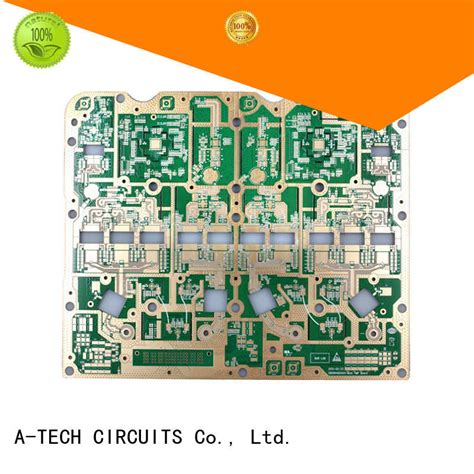
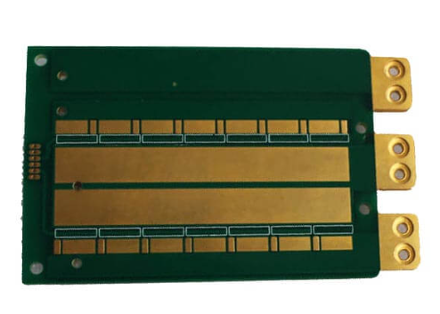
Printed Circuit Boards (PCBs) are the backbone of modern electronic devices, serving as the foundation upon which electronic components are mounted and interconnected. Understanding the basics of industrial PCB manufacturing is essential for appreciating the complexity and precision involved in creating these critical components.
The process begins with the design phase, where engineers use specialized software to create a schematic diagram and layout of the PCB.
This design is then translated into a format that can be used for manufacturing, typically a Gerber file, which contains all the necessary information about the board’s layers, traces, and component placements.
Once the design is finalized, the manufacturing process commences with the selection of the base material, usually a fiberglass-reinforced epoxy laminate known as FR-4.
This material is chosen for its excellent electrical insulation properties and mechanical strength. The next step involves the application of a thin layer of copper to both sides of the substrate, which will form the conductive pathways of the PCB. This is achieved through a process called lamination, where heat and pressure are applied to bond the copper to the substrate.
Following lamination, the board undergoes a process known as photolithography.
During this stage, a photosensitive film, or photoresist, is applied to the copper-clad board. The board is then exposed to ultraviolet light through a mask that represents the circuit pattern. The areas exposed to light harden, while the unexposed areas remain soft and are subsequently removed using a chemical solution. This leaves behind a precise pattern of copper traces that will form the electrical connections on the PCB.
The next phase involves etching, where the excess copper is removed from the board.
This is typically done using a chemical solution that dissolves the unwanted copper, leaving only the desired circuit pattern intact. After etching, the board is cleaned to remove any residual chemicals and debris. At this point, the board may undergo additional processes such as drilling, where holes are created for component leads and vias, which are used to connect different layers of the PCB.
Once the board is drilled, it is plated with a thin layer of metal, usually copper, to ensure electrical connectivity between layers.
This is followed by the application of a solder mask, a protective layer that prevents solder from bridging between conductive traces and causing short circuits. The solder mask also provides a surface for the application of silkscreen, which is used to print component labels and other identifying information on the board.
The final stages of PCB manufacturing involve testing and quality control.
Each board is subjected to rigorous electrical testing to ensure that all connections are correct and that there are no short circuits or open circuits. This is often done using automated test equipment that can quickly and accurately verify the integrity of the board. Once testing is complete, the boards are inspected for any physical defects and are then packaged for shipment.
In conclusion, the industrial PCB manufacturing process is a complex and highly precise operation that involves multiple stages, each critical to the production of reliable and high-quality PCBs. From design to testing, each step requires careful attention to detail and adherence to strict quality standards to ensure that the final product meets the demands of modern electronic applications. Understanding these basics provides insight into the intricate world of PCB manufacturing and the essential role it plays in the electronics industry.
Key Steps In The PCB Fabrication Process
The industrial PCB manufacturing process is a complex and intricate procedure that involves several key steps, each crucial to the creation of a functional printed circuit board. Understanding these steps provides insight into how electronic devices are brought to life, from the initial design to the final product.
The process begins with the design phase, where engineers use specialized software to create a detailed blueprint of the PCB.
This design includes the layout of the circuit, the placement of components, and the routing of electrical connections. Once the design is finalized, it is converted into a format suitable for manufacturing, typically a Gerber file, which serves as a guide for the subsequent fabrication steps.
Following the design phase, the next step is the preparation of the substrate, which forms the base of the PCB.
The substrate is usually made of a non-conductive material such as fiberglass, which provides structural support. A thin layer of copper is then laminated onto the substrate, forming the conductive pathways that will carry electrical signals. This copper layer is crucial, as it will be etched away in later steps to create the desired circuit pattern. The substrate is then cleaned and prepared for the application of a photosensitive resist, which is essential for the photolithography process.
Photolithography is a critical step in PCB fabrication, as it defines the circuit pattern on the copper layer.
During this process, the photosensitive resist is exposed to ultraviolet light through a mask that contains the circuit design. The exposed areas of the resist harden, while the unexposed areas remain soft and are subsequently washed away. This leaves a precise pattern of resist on the copper layer, which protects certain areas during the etching process. The board is then subjected to an etching solution, which removes the unprotected copper, leaving behind the desired circuit pattern.
Once the etching is complete, the next step is drilling, where holes are created for component leads and vias, which are used to connect different layers of the PCB.
Precision drilling machines are employed to ensure accuracy, as even minor deviations can affect the board’s functionality. After drilling, the board undergoes a plating process, where a thin layer of copper is deposited onto the walls of the drilled holes, establishing electrical connections between layers.
The subsequent step involves the application of a solder mask, which is a protective layer that insulates the copper traces and prevents solder bridges during component assembly.
The solder mask is typically green, although other colors are available, and is applied using a similar photolithographic process as before. Once the solder mask is in place, a silkscreen layer is added, which contains labels and markings to assist in component placement and identification.
Finally, the PCB undergoes a series of inspections and tests to ensure its quality and functionality.
Automated optical inspection (AOI) systems are used to detect any defects in the circuit pattern, while electrical tests verify the board’s performance. Once the PCB passes these tests, it is ready for assembly, where components are soldered onto the board to create a complete electronic device. Through these meticulous steps, the industrial PCB manufacturing process transforms a simple design into a sophisticated and essential component of modern technology.

Innovations In PCB Manufacturing Technology
In recent years, the industrial PCB manufacturing process has witnessed significant innovations, driven by the relentless pursuit of efficiency, precision, and sustainability. These advancements have not only enhanced the quality and functionality of printed circuit boards but have also streamlined production processes, thereby reducing costs and environmental impact.
One of the most notable innovations in PCB manufacturing technology is the adoption of advanced materials.
Traditional materials like FR-4 are increasingly being supplemented or replaced by high-performance substrates such as polyimide and ceramic-based materials. These materials offer superior thermal stability and electrical performance, which are crucial for the ever-evolving demands of modern electronic devices. Consequently, manufacturers can produce PCBs that are more reliable and capable of supporting higher frequencies and power densities.
In addition to material advancements, the integration of automation and robotics has revolutionized the PCB manufacturing landscape.
Automated systems now handle tasks ranging from drilling and plating to inspection and testing, significantly reducing human error and increasing production speed. Robotics, in particular, have enabled precise and consistent execution of complex processes, ensuring that each PCB meets stringent quality standards. This shift towards automation not only enhances productivity but also allows manufacturers to respond swiftly to market demands, thereby maintaining a competitive edge.
Moreover, the advent of additive manufacturing, commonly known as 3D printing, has introduced a new dimension to PCB production.
This technology allows for the creation of complex, multi-layered circuit boards with intricate designs that were previously challenging to achieve using traditional subtractive methods. By building PCBs layer by layer, manufacturers can optimize material usage and reduce waste, aligning with the growing emphasis on sustainable practices. Furthermore, 3D printing facilitates rapid prototyping, enabling designers to iterate and refine their designs quickly, thus accelerating the development cycle.
Another significant innovation is the implementation of advanced imaging and inspection technologies.
High-resolution imaging systems, such as automated optical inspection (AOI) and X-ray inspection, have become integral to the quality assurance process. These technologies provide detailed insights into the structural integrity of PCBs, allowing for the early detection of defects and anomalies. As a result, manufacturers can ensure that only boards meeting the highest standards reach the market, thereby enhancing product reliability and customer satisfaction.
Furthermore, the rise of digital twin technology has introduced a paradigm shift in PCB manufacturing.
By creating a virtual replica of the physical PCB, manufacturers can simulate and analyze various scenarios, optimizing design and production processes before actual fabrication. This predictive capability not only reduces the likelihood of errors but also minimizes the need for costly rework and adjustments. Consequently, digital twins contribute to more efficient and cost-effective manufacturing operations.
In conclusion, the industrial PCB manufacturing process has undergone transformative changes, driven by innovations in materials, automation, additive manufacturing, imaging technologies, and digital twins. These advancements have collectively enhanced the efficiency, precision, and sustainability of PCB production, enabling manufacturers to meet the increasing demands of modern electronics. As technology continues to evolve, it is anticipated that further innovations will emerge, propelling the PCB manufacturing industry towards even greater heights of excellence and innovation.
Quality Control Measures In PCB Production
In the realm of industrial PCB manufacturing, quality control measures are paramount to ensuring the reliability and functionality of printed circuit boards.
As the backbone of modern electronic devices, PCBs must adhere to stringent quality standards to meet the demands of various industries, from consumer electronics to aerospace. The quality control process in PCB production is multifaceted, encompassing several stages that collectively ensure the final product meets the required specifications and performance criteria.
Initially, the quality control process begins with the design phase, where engineers utilize advanced software tools to create precise and error-free PCB layouts.
This stage is crucial, as any design flaws can lead to significant issues during manufacturing. Design rule checks (DRC) are employed to verify that the layout adheres to the manufacturing capabilities and constraints, thereby minimizing the risk of defects in the subsequent stages.
Following the design phase, the focus shifts to the selection of materials.
High-quality substrates, copper foils, and laminates are chosen based on the specific requirements of the PCB application. Material inspection is a critical quality control measure, as it ensures that the raw materials meet the necessary standards for durability, conductivity, and thermal resistance. By conducting thorough inspections, manufacturers can prevent potential issues that may arise from substandard materials.
As the manufacturing process progresses, the etching stage is another critical point for quality control.
During etching, unwanted copper is removed to create the desired circuit patterns. Precision is essential here, as any deviation can lead to short circuits or open circuits. Automated optical inspection (AOI) systems are employed to detect any discrepancies in the etched patterns, allowing for immediate corrective actions.
Subsequently, the solder mask application and silkscreen printing stages require meticulous attention to detail.
The solder mask serves as a protective layer, preventing solder bridges and corrosion, while the silkscreen provides essential labeling for component placement. Quality control measures at this stage involve verifying the alignment and thickness of the solder mask and ensuring the clarity and accuracy of the silkscreen print. Any errors detected are rectified to maintain the integrity of the PCB.
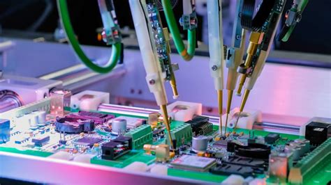
The assembly process introduces another layer of complexity, as components are mounted onto the PCB.
Surface mount technology (SMT) and through-hole technology (THT) are commonly used methods, each requiring precise placement and soldering of components. Automated pick-and-place machines, coupled with AOI and X-ray inspection systems, are employed to ensure that components are correctly positioned and soldered. These technologies help identify misalignments, missing components, or soldering defects, which can then be addressed promptly.
Finally, functional testing is conducted to verify the performance of the assembled PCB.
This involves subjecting the board to various electrical tests to ensure it operates as intended under different conditions. In-circuit testing (ICT) and functional testing are standard practices that help identify any latent defects that may have been overlooked in earlier stages. By rigorously testing the PCBs, manufacturers can guarantee that only fully functional boards are delivered to customers.
In conclusion, quality control measures in PCB production are integral to the manufacturing process, ensuring that each board meets the highest standards of reliability and performance. From design verification to material inspection, and from precision etching to comprehensive testing, every stage is meticulously monitored and controlled. These measures not only enhance the quality of the final product but also reinforce the trust and confidence that industries place in PCB manufacturers.