Innovations in Assembled Printed Circuit Boards for Modern Electronics

Key Takeaways
In the rapidly evolving landscape of electronics, assembled printed circuit boards (PCBs) have emerged as a cornerstone of innovation. The transition from traditional manufacturing to advanced pcb assembly techniques has paved the way for improved performance and efficiency. One of the most significant takeaways is the importance of design innovations that enhance the functionality and compatibility of pcba with various electronic devices. Furthermore, advancements in materials are transforming pcb assembly, allowing for lighter, more durable, and thermally efficient boards that better meet the demands of modern technology.
It is crucial to recognize that streamlining manufacturing processes not only reduces production time but also minimizes costs associated with waste and material usage. The integration of automation technology into pcb assembly is another vital trend, enabling precision and scalability in production without compromising quality. As these trends continue to develop, environmental considerations are becoming increasingly important, with designers focusing on sustainability in their pcba designs.
"The future of electronics lies in our ability to innovate while being mindful of our environmental impact."
This holistic approach not only fosters creativity but also builds resilience into manufacturing practices, ensuring that modern electronics can adapt swiftly to changing market demands while adhering to sustainable standards. Keeping an eye on these key aspects will empower manufacturers and designers alike to stay ahead in the competitive realm of assembled printed circuit boards.

The Evolution of Assembled Printed Circuit Boards: A Historical Perspective
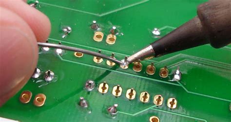
The history of assembled printed circuit boards (PCBs) is a testament to the relentless pursuit of innovation within the electronics industry. Beginning in the early 20th century, pcb assembly processes evolved from simple wire connections to the sophisticated techniques we see today. Initially, PCBs were manually assembled, with components painstakingly soldered by hand. However, as technology advanced, this labor-intensive approach was gradually replaced by more precise and efficient methods.
In the 1960s and 1970s, the introduction of automated assembly technologies marked a significant turning point in pcba practices. This shift towards automation not only expedited production but also dramatically improved reliability and consistency in solder joints. The move from through-hole to surface mount technology (SMT) further revolutionized PCBs, allowing for a significant reduction in size while increasing component density.
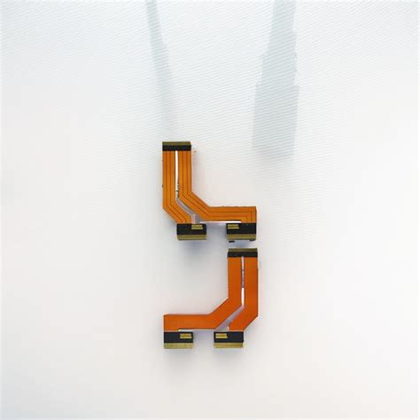
Over time, materials used in PCB manufacturing have also seen substantial innovation. Advances in materials technology have led to PCBs that are not only lighter and more cost-effective but also capable of operating at higher frequencies and temperatures. For example, the development of flexible printed circuit boards (FPCBs) allows for dynamic applications that can bend and adapt to various environments.
The table below summarizes key milestones in pcb assembly evolution:
| Year | Milestone | Impact |
|---|---|---|
| 1943 | First use of PCBs | Introduction of compact circuit designs |
| 1960s | Automated assembly introduced | Enhanced production speed and reliability |
| 1980s | Adoption of SMT | Increased component density |
| 1990s | Emergence of FPCBs | Flexibility in electronic device design |
As we continue into the 21st century, the evolution of assembled printed circuit boards remains ongoing. Each innovation contributes to enhanced performance capabilities across a multitude of devices—from smartphones to aerospace applications—reflecting a continuous journey toward greater efficiency and effectiveness in modern electronics.

Key Design Innovations in Assembled Printed Circuit Boards
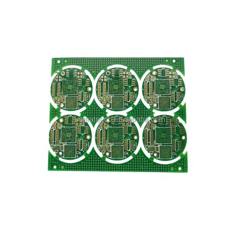
In the realm of pcb assembly, significant design innovations are reshaping the landscape of modern electronics. With the increasing demand for compact and efficient devices, advancements in PCB design techniques have led to a remarkable shift towards multilayered printed circuit boards (PCBs). These multilayer designs optimize space while enhancing electrical performance, allowing for increased functionality within smaller footprints. Additionally, new methodologies such as design for manufacturability (DFM) are being employed to streamline pcba processes, thereby reducing production costs and time-to-market.
Another pivotal innovation is the implementation of high-density interconnect (HDI) technology, which utilizes finer traces and spaces between components to improve signal integrity and reduce electromagnetic interference. This technology not only increases the performance of the assembled printed circuit boards but also supports a higher component density, aiding in the development of more complex electronic systems.
Moreover, advancements in computer-aided design (CAD) tools have facilitated more intricate designs and simulations before actual manufacturing begins. This ensures that potential errors can be identified and mitigated early in the process, resulting in a more reliable final product. The integration of smart manufacturing principles within pcb assembly workflows is also noteworthy; this includes real-time monitoring and feedback loops that enhance production reliability.
These key design innovations are crucial as they not only improve performance but also pave the way for future technologies that rely on increasingly sophisticated assembled printed circuit boards. The ongoing evolution of these design techniques signifies a profound change in how electronic devices are envisioned and produced today.
Advanced Materials Revolutionizing PCB Performance
The performance of assembled printed circuit boards (PCBs) is greatly impacted by the emergence of advanced materials that enhance functionality, durability, and reliability. Innovations in materials science have led to the development of high-frequency substrates, which are crucial for the performance of next-generation electronics. These substrates, composed of low-loss dielectric materials, enable efficient signal transmission and support higher operating frequencies, making them indispensable in the fields of telecommunications and computing. Moreover, advancements in soldering materials, such as lead-free solders with improved thermal and mechanical properties, contribute to better adhesion and reliability during the PCB assembly process. Additionally, flexible printed circuit boards (FPCBs) often incorporate materials that provide both mechanical flexibility and electrical performance advantages, expanding their applicability in consumer electronics and wearable devices. The integration of novel thermally conductive materials also aids in heat dissipation, thereby preventing overheating in compact electronic systems. Collectively, these innovative materials are pivotal not only in enhancing the pcba process but also ensuring that modern devices continue to meet increasing performance demands while staying aligned with sustainability goals. As the industry progresses, it is clear that these advanced materials will play a vital role in shaping the future landscape of assembled printed circuit boards.
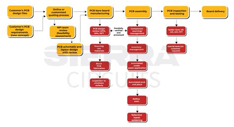
Streamlining Manufacturing Processes for Efficient PCB Production
The production of assembled printed circuit boards (PCBs) has undergone significant transformation through advanced manufacturing processes that aim to enhance efficiency and reduce costs. In the current landscape, pcb assembly is increasingly automated, utilizing sophisticated machines to streamline operations. This automation not only accelerates the manufacturing timeline but also minimizes human error, ensuring a higher quality of output in the pcb assembly line. Innovations such as selective soldering and pick-and-place technology contribute to this efficiency, allowing for precise placement of components on PCBs, which is essential for optimizing performance and reliability in modern electronics.
Moreover, the integration of data analytics and real-time monitoring during the PCBA processes enables manufacturers to continuously optimize their operations. By analyzing data collected during production, companies can identify bottlenecks and inefficiencies quickly. As a result, manufacturers are able to adapt their processes dynamically, leading to improved resource allocation and reduced waste. The emphasis on lean manufacturing principles further complements these advancements by striving to eliminate non-value-adding steps in production.
In conclusion, streamlining the manufacturing processes for assembled printed circuit boards is vital for enhancing both productivity and performance in the electronics industry. The shift towards automation combined with data-driven approaches not only supports faster turnaround times but also ensures that high standards are maintained throughout pcb assembly, thereby meeting the growing demands for sophisticated electronic devices.
The Role of Automation in Modern PCB Assembly
The integration of automation in modern pcb assembly has fundamentally transformed the landscape of printed circuit board (PCBA) manufacturing. As the demand for higher efficiency and precision in electronics escalates, automated systems have become indispensable. Automation not only accelerates the assembly process but significantly reduces human error, ensuring that each component is placed with unparalleled accuracy. State-of-the-art technologies, such as robotic soldering and advanced pick-and-place machinery, exemplify how automation enhances both speed and quality in pcba production. Furthermore, automated inspection systems are now employed to identify defects early in the manufacturing process, allowing for timely corrections and minimizing waste. This shift towards automation has also enabled manufacturers to scale operations rapidly, accommodating the growing complexity of modern electronics. In this context, automation serves not merely as a tool for efficiency; it is a catalyst for innovation, paving the way for advanced designs and applications that were previously unattainable. As we progress further into an era marked by smart devices and intricate circuitry, the role of automation in pcb assembly will undoubtedly expand, driving the next wave of innovations in this critical field.

Environmental Considerations in Assembled Printed Circuit Board Design
In today’s rapidly evolving electronics landscape, environmental considerations have gained paramount importance in the design of assembled printed circuit boards (PCBs). The pcb assembly process must now prioritize sustainability to mitigate the impact on our planet. This entails using eco-friendly materials that reduce toxic waste and energy consumption during production. For instance, adopting lead-free soldering techniques not only complies with rigorous environmental regulations but also enhances the overall safety of the devices we rely on daily. Furthermore, the integration of design for manufacturing (DFM) principles encourages more efficient layouts and reduces unnecessary material usage, subsequently minimizing waste. Innovative approaches such as circular economy practices are also gaining traction, allowing for the recycling and repurposing of pcba components at the end of their lifecycle. By embedding these principles into PCB design and manufacturing processes, manufacturers can significantly lower their carbon footprint while maintaining high performance standards, ultimately leading to more sustainable electronic solutions for the future.
Future Trends in Assembled Printed Circuit Board Technologies
As the landscape of modern electronics continues to evolve, the future of assembled printed circuit boards (PCBs) is poised for transformative changes driven by innovation. One prominent trend is the increasing integration of flexible and rigid-flex PCBs, which offer significant advantages in compact designs and adaptability. These technologies enable more complex circuit layouts while minimizing the overall form factor, thereby enhancing device portability. Additionally, advancements in pcb assembly techniques are paving the way for greater precision and reliability. The utilization of automated assembly processes, such as pick-and-place machinery, ensures that components are positioned accurately, reducing the risk of defects and enabling higher throughput rates.
Moreover, environmental sustainability is becoming a focal point for pcba practices. The demand for eco-friendly materials and manufacturing processes is leading to innovations such as biodegradable substrates and lead-free soldering techniques. Such initiatives not only comply with regulatory standards but also align with consumer preferences for environmentally responsible products.
Another significant trend is the incorporation of smart technologies into PCB design, allowing for enhanced functionality through embedded sensors and wireless connectivity solutions. This connectivity integrates seamless communication between devices, bringing about a more interconnected consumer experience.
In summary, as we look ahead to the future trends in assembled printed circuit board technologies, it’s clear that continued innovation in materials, design practices, and production methods will play a critical role in shaping next-generation electronic devices that are efficient, sustainable, and user-friendly.
Case Studies: Successful Implementations of Innovative PCBs in Electronics
In recent years, numerous companies have successfully adopted assembled printed circuit boards (PCBs) with innovative designs, leading to remarkable improvements in electronic devices. For instance, a leading smartphone manufacturer revamped its product line by integrating flexible PCBs that allow for sophisticated layouts and reduced space in design. This transition not only contributed to a slimmer profile but also enhanced the performance of the phone, allowing for better heat dissipation and improved battery life. Another noteworthy example can be seen in the automotive industry, where pcb assembly has evolved to incorporate high-frequency applications. A prominent electric vehicle company utilized pcba technologies to create reliable and efficient PCBs that support advanced driver-assistance systems (ADAS), significantly enhancing vehicle safety and functionality. Furthermore, a well-known consumer electronics brand embarked on a project focused on utilizing eco-friendly materials in its assembled printed circuit boards, resulting in both improved performance metrics and reduced environmental impact. These cases illustrate how innovative approaches to PCB assembly not only adhere to modern aesthetic and functional demands but also pave the way for future advancements in various sectors of electronics.
Conclusion
As the landscape of electronics continues to evolve, the innovations in assembled printed circuit boards (PCBs) play a pivotal role in driving performance and efficiency. The advancements in pcb assembly techniques, combined with the introduction of new materials and design enhancements, have transformed how electronic devices are conceptualized and manufactured. The integration of automation into the pcba process has not only streamlined production but has also significantly reduced human error, leading to higher quality end products. Consequently, these progressions contribute to the overall longevity and reliability of electronic systems. Furthermore, addressing environmental concerns through eco-friendly materials and practices within PCB design emphasizes the industry’s commitment to sustainability. As we look toward the future, it is clear that ongoing research and development will continue to shape assembled printed circuit boards, ensuring they meet the ever-growing demands of modern electronics while maintaining their foundational role in technological advancement.
FAQs
What is PCB assembly?
PCB assembly, often abbreviated as PCBA, refers to the process of soldering electronic components onto a printed circuit board, effectively integrating various electronic parts into a single functional unit.
What are the key innovations in assembled printed circuit boards?
Recent innovations in assembled printed circuit boards include enhanced designs that improve thermal management, the use of advanced materials that increase durability, and manufacturing processes that enhance precision and efficiency.
How does automation contribute to modern PCB assembly?
Automation significantly enhances PCB assembly by reducing human errors, increasing production speed, and enabling high-quality output through standardized processes. This leads to more consistent results in pcba while optimizing labor costs.
What materials are commonly used in modern PCBs?
The latest advancements have introduced materials such as high-frequency laminates, flexible substrates, and environmentally friendly solder options that improve overall performance and sustainability in pcb assembly.
How do environmental concerns affect PCB design?
Designers are increasingly considering eco-friendly practices during the pcb assembly process. This includes using recyclable materials, reducing waste throughout the manufacturing phases, and ensuring compliance with global environmental standards.
Explore More About PCB Assembly
For more insights on innovations in pcb assembly, please click here.