Innovations in PCB Design and Manufacturing for Modern Electronics
Key Takeaways
The advancements in PCB design and manufacturing reflect significant progress that shapes the future of modern electronics. As we delve into the current trends, it’s crucial to recognize that the integration of advanced technologies has fundamentally transformed PCB assembly processes, improving efficiency and outcomes. The incorporation of intelligent automation tools enhances precision in PCBA, leading to reduced human intervention and minimal errors during production. Furthermore, the use of innovative materials contributes greatly to the performance attributes of printed circuit boards, ensuring they can withstand demanding applications. Additionally, sustainable practices are increasingly being integrated into design processes, promoting eco-friendliness while maintaining high standards of quality. With the aid of sophisticated software solutions, designers are now capable of simulating and optimizing designs more effectively than ever before. Understanding these key aspects will equip stakeholders with insights necessary to navigate the evolving landscape and harness opportunities in a competitive industry, reinforcing the importance of keeping abreast with innovations surrounding pcb assembly and pcba methodologies.
Introduction to PCB Design and Manufacturing Innovations
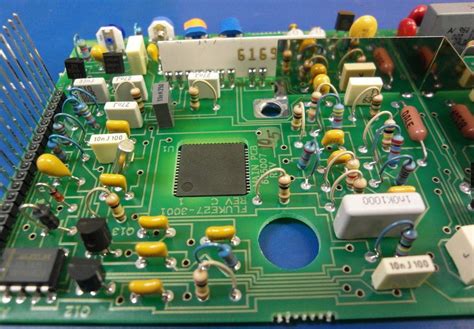
The world of electronics is experiencing transformative changes, particularly in PCB design and manufacturing. These innovations play a pivotal role in developing advanced electronic devices that are faster, more efficient, and tailored to meet the demands of modern technology. Central to this evolution is pcb assembly, or PCBA, where a meticulously designed circuit board incorporates a variety of components to create functional electronic systems. As the demand for smaller, lighter, and more powerful devices rises, industries are progressively adopting methods like surface-mount technology (SMT) and advanced soldering techniques to optimize the pcb assembly process.
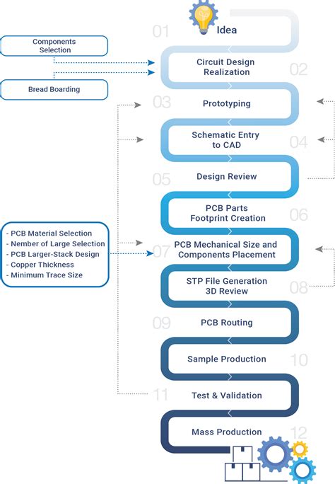
Moreover, integrating state-of-the-art tools such as computer-aided design (CAD) software has revolutionized the way engineers visualize and test their PCB layouts before mass production. This technology not only facilitates precision but also accelerates the prototyping phase significantly, ensuring that products reach the market in record time.
“Innovation is at the heart of competitive advantage; it’s not just about keeping pace with technology but about leading it.”
As manufacturers embrace automation in their production lines, we witness substantial reductions in human error and faster turnaround times—demonstrating that modern innovations in PCB manufacturing not only enhance performance but also streamline processes for greater efficiency. In summary, the continuous advancements in PCB design methods and manufacturing technologies are essential for meeting the relentless pace of electronic innovation, ensuring sustainability and excellence at every stage of production.
Key Technologies Transforming PCB Production
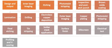
The landscape of PCB design and manufacturing is undergoing a remarkable transformation, largely driven by technological advancements that enhance performance and improve production efficiency. One of the most significant innovations is the use of advanced materials that not only optimize thermal and electrical characteristics but also allow for thinner, lighter boards. This is particularly essential in the realm of consumer electronics, where space is at a premium. Additionally, automation technologies are increasingly being implemented in the PCB assembly process. The integration of robotics and AI-driven machinery can minimize human error while significantly speeding up assembly lines, converting them into intelligent systems capable of adapting to various production demands seamlessly.
Moreover, the application of sophisticated software tools in modern PCB design has made it easier for engineers to create intricate layouts while also simulating performance outcomes before actual PCBA takes place. These tools can analyze factors such as signal integrity, thermal performance, and electromigration to ensure that the final product adheres to high-quality standards. Furthermore, advancements in manufacturing techniques, including additive manufacturing or 3D printing, have opened new avenues for creating complex geometries that were previously impractical with traditional methods.
As industries become more conscious of their environmental footprint, integrating sustainable practices into PCB production has become imperative. Innovations such as eco-friendly materials and processes not only align with regulatory requirements but also meet growing consumer demand for green products. Ultimately, these key technologies are redefining the status quo in PCB design and manufacturing, allowing companies to maintain a competitive edge while meeting the rigorous demands of modern electronics.
Advanced Materials and Their Impact on PCB Performance
The integration of advanced materials in PCB design and manufacturing has significantly elevated the performance and reliability of modern electronics. As the demand for higher functionality and miniaturization in devices increases, engineers are turning to innovative materials that enhance signal integrity and thermal management. For instance, high-frequency laminates provide superior electrical properties which are essential for applications like 5G and high-speed data processing. These materials can withstand elevated operating frequencies while minimizing signal loss, which is critical in maintaining communication efficiency in advanced applications.
Another important aspect is the utilization of metal-core PCBs (MCPCBs), which feature a conductive metal substrate that effectively dissipates heat. This property is particularly beneficial in high-power applications such as LED technology, where heat management is crucial for longevity and performance. Additionally, advancements in dielectric materials have led to a reduction in board thickness without compromising electrical performance, resulting in lighter and more compact designs.
Moreover, the process of PCB assembly (PCBA) benefits from these innovative materials as they enable more robust connections between components, ultimately leading to lower failure rates. The selection of appropriate materials not only impacts the performance but also influences production efficiency—certain materials can enhance solder flow during assembly, leading to higher-quality products.
In summary, embracing advanced materials is pivotal for achieving enhanced productivity and reliability within the ever-evolving landscape of electronics manufacturing.
| Material Type | Key Benefits | Applications |
|---|---|---|
| High-Frequency Laminates | Improved signal integrity | 5G technology, RF applications |
| Metal-Core PCBs | Effective heat dissipation | LED technology, high-power devices |
| Innovative Dielectrics | Reduced board thickness | Consumer electronics |
In conclusion, it’s clear that selecting the right advanced materials isn’t just about meeting current demands; it’s about anticipating future challenges faced in PCB design and production. By investing in these innovative resources, manufacturers can ensure a competitive edge by enhancing overall product performance while streamlining manufacturing processes.
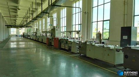
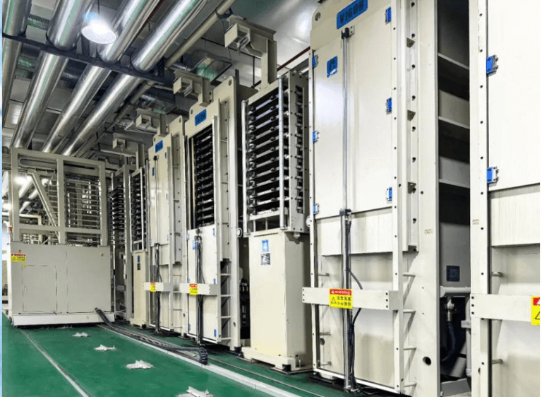
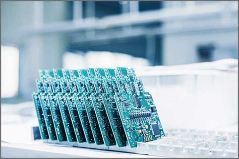
Automation in PCB Manufacturing: Revolutionizing the Process
Automation has emerged as a pivotal factor in enhancing the PCB assembly and manufacturing processes, effectively transforming how electronics are produced. By integrating advanced robotics and automated machinery, manufacturers can achieve unprecedented levels of efficiency and precision in PCBA. These technologies streamline repetitive tasks such as component placement, soldering, and inspection, thus reducing the likelihood of human error. Furthermore, automation facilitates faster production cycles, which is essential in meeting the growing demand for rapid turnaround times in the modern electronics industry. The implementation of smart manufacturing technologies, such as data analytics and machine learning, allows for real-time monitoring and optimization of production lines. As a result, manufacturers not only enhance their productivity but also improve the quality and reliability of their PCB products. This drive toward automation is not merely a trend; it encapsulates the future of PCB design and manufacturing as companies seek to maintain a competitive edge while adapting to evolving market needs.
Sustainable Practices in PCB Design and Production
As the electronics industry evolves, there is an increasing emphasis on incorporating sustainable practices into PCB design and production. Companies are now recognizing the environmental impact of traditional methods and are actively seeking alternatives that reduce waste and enhance energy efficiency. The use of lead-free solder and environmentally friendly materials in PCB assembly not only minimizes toxicity but also aligns with global regulations aimed at reducing harmful substances in electronics. Moreover, implementing recycling programs for discarded boards helps recover valuable materials, significantly lowering the demand for virgin resources. By adopting modular designs, manufacturers can improve the repairability and upgradeability of products, which extends the lifecycle of electronic devices and decreases overall waste. In this context, the integration of digital technologies in the manufacturing process facilitates better monitoring of resources, enabling more efficient production workflows—ultimately leading to a smaller carbon footprint. As we look toward the future, embracing sustainable methodologies in PCBA is not just a trend; it represents a crucial pivot towards environmentally responsible manufacturing that benefits both businesses and the planet alike.
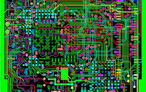
The Role of Software in Modern PCB Design
In today’s fast-paced electronics industry, the significance of software in PCB design cannot be overstated. Modern PCB design software solutions have transformed traditional methods, enabling engineers to create intricate layouts with precision and efficiency. Through the integration of advanced algorithms and automated tools, these platforms enhance the design process, allowing for rapid prototyping and iterative testing. This is particularly crucial in PCB assembly (PCBA), where errors in the design phase can lead to costly manufacturing setbacks. The ability to simulate how a PCB will perform under various conditions provides invaluable insights, helping designers make informed decisions early in the process. Furthermore, collaborative features enable multiple stakeholders to contribute in real time, streamlining communication and improving project timelines. These technological advancements not only reduce production costs but also enhance the overall quality and reliability of final products, giving companies a tangible competitive edge in an increasingly challenging market. With such comprehensive software tools at their disposal, engineers are better equipped than ever to tackle complex designs while adhering to stringent regulatory and performance standards.
Challenges and Solutions in the Evolving PCB Landscape
As pcb design and manufacturing continue to advance, the industry faces a multitude of challenges that require innovative solutions. One of the primary challenges is managing the increasing complexity of modern PCBs, which necessitates higher precision in pcb assembly processes. With demands for smaller, more compact electronic devices, manufacturers are often pushed to produce PCBA that incorporate finer details and tighter spaces. This complexity can lead to issues such as thermal management and signal integrity, impacting overall performance. To address these challenges, companies are investing in advanced materials that offer better thermal conductivity and support efficient signal transmission. Furthermore, the adoption of automation and smart manufacturing technologies is becoming essential for streamlining production processes and reducing human error. Implementing robust quality control measures ensures that any potential defects in pcb assembly are detected early in the production cycle, thus maintaining high standards of quality. As these challenges evolve, so do the solutions, highlighting a dynamic landscape where innovation is key to sustainability and competitiveness in the PCB manufacturing sector.
Future Trends in PCB Manufacturing for Next-Gen Electronics
As the electronics industry continues to evolve, the landscape of PCB design and manufacturing is set to undergo significant transformations. One of the most notable trends is the increasing integration of advanced materials, such as flexible substrates and high-frequency laminates, which enhance the performance and reliability of printed circuit boards (PCBs). These materials not only improve signal integrity but also allow for more compact and lightweight designs, essential for modern devices. Additionally, automation in PCB assembly (PCBA) processes is becoming vital. This shift towards automated solutions helps streamline production workflows, reduce human error, and improve efficiency, making it easier for manufacturers to meet the rising demand for more complex electronic products.
Moreover, the implementation of smart manufacturing technologies, including the Internet of Things (IoT) and artificial intelligence (AI), is revolutionizing how PCBs are produced. These technologies facilitate real-time monitoring and predictive maintenance of equipment, ensuring optimal performance and reducing downtime during production. As environmental concerns grow, sustainable practices are also gaining prominence in PCB manufacturing. Efforts to recycle materials and minimize waste are becoming integral components of modern production strategies. Thus, as we look to the future, these trends—innovative materials, automation in PCBA, smart manufacturing technologies, and sustainable practices—are collectively shaping a more efficient and environmentally responsible PCB landscape for next-generation electronics.
Conclusion
In the rapidly evolving world of electronics, the importance of PCB design and manufacturing cannot be overstated. The integration of innovative technologies has not only refined traditional methods but also introduced new paradigms for efficiency and performance. Key advancements in pcb assembly, or PCBA, have propelled the capability to produce increasingly complex designs while ensuring reliability and durability. With a focus on advanced materials, manufacturers are now able to improve electrical performance and thermal management, directly impacting the longevity of electronic devices. Moreover, automation has emerged as a game changer in PCB manufacturing, streamlining processes and reducing time-to-market. The role of software in this arena cannot be overlooked, as it facilitates intricate design processes while enabling simulations that predict performance outcomes before production. Embracing sustainable practices also plays a crucial role in modern production, addressing environmental concerns while fulfilling regulatory demands. As we look towards the future, these innovations will undoubtedly continue to shape the landscape of electronics, making them more efficient and reliable than ever before. The interplay between technology and creativity in PCB design ensures that manufacturers are well-equipped to meet the demands of next-generation applications, solidifying their competitive edge in this dynamic industry.
FAQs
What is PCB assembly?
PCB assembly, commonly referred to as PCBA, is the process of soldering electronic components onto a printed circuit board (PCB) to create a functional assembly. This critical step transforms a bare PCB into a complete electronic product.
What are the benefits of PCBA in modern electronics?
The benefits of PCBA include enhanced performance, improved reliability, and shorter production cycles. By utilizing advanced techniques in PCB design and manufacturing, products can achieve greater efficiency and durability.
How has automation impacted PCB assembly?
Automation has revolutionized pcb assembly by significantly increasing production speed and accuracy. Automated processes minimize human error and ensure consistent quality, enabling manufacturers to meet growing demands in a competitive market.
What are common challenges in PCB design?
Some challenges in pcb design and manufacturing involve managing heat dissipation, signal integrity, and minimizing space for components. Innovations in materials and design techniques are helping to address these issues effectively.
Why is material selection important in PCB manufacturing?
Material selection plays a crucial role in determining the performance characteristics of the PCB assembly, influencing factors such as thermal conductivity, electrical performance, and overall durability. Selecting high-quality materials can lead to better long-term reliability.