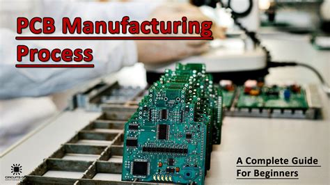
Innovations in PCB Manufacturing and Assembly for Modern Electronics

Key Takeaways
The landscape of PCB assembly and manufacturing continues to evolve significantly, driven by the relentless pursuit of efficiency and reliability in modern electronics. Several key innovations have emerged in recent years, fundamentally altering traditional techniques. Automation and robotics are now essential components in this sector, allowing for increased precision and reduced production times, leading to a more streamlined PCBA process. Furthermore, the introduction of cutting-edge materials enhances the durability and performance of printed circuit boards. For example, flexible PCBs are gaining traction due to their adaptability and lightweight properties.
Tables illustrating advancements in materials and their impact on performance are becoming common tools for manufacturers to convey complex information simply and effectively.
“The integration of innovative materials not only improves performance but also opens up new possibilities for circuit design,” emphasizes one industry expert.
As we focus on procedural advancements, technologies such as additive manufacturing play a crucial role in enhancing fabrication processes. Particularly noteworthy is how these changes result in reduced waste material usage—a key aspect of sustainable practices integral to the future of PCB manufacturing.
In summary, these takeaways reflect how modernization is steering the industry toward smarter, more resilient practices while underscoring the critical importance of innovation in supporting the evolving demands of electronic applications.
The Evolution of PCB Manufacturing Techniques
The landscape of PCB manufacturing has undergone significant transformations over the decades, adapting to the fast-paced demands of modern technology. Initially, the processes relied heavily on manual labor and rudimentary methods, which were time-consuming and prone to errors. However, with the advent of digital technology and improved design tools, PCB assembly has become more streamlined. Modern approaches utilize advanced software for design verification, ensuring that each circuit layout is optimized before production begins.
Furthermore, innovations such as Surface Mount Technology (SMT) have dramatically altered the assembly process. SMT allows components to be mounted directly onto the surface of PCBs rather than being placed through holes, which saves space and improves performance. This shift has led to a new era in pcba efficiency by enabling denser circuit designs that maximize functionality without increasing size.
In addition to improved methods, new materials are being introduced into manufacturing processes. High-frequency substrates and flexible laminates are becoming common in high-performance applications, catering specifically to the demands of 5G technology and IoT devices.
As we look towards the future, it’s clear that ongoing advancements in automation and robotics will continue to refine PCB production, lowering costs while enhancing quality and reliability. The evolution we observe is not merely a progression but a revolutionary shift towards more innovative practices in pcba that will define the next generation of electronics.
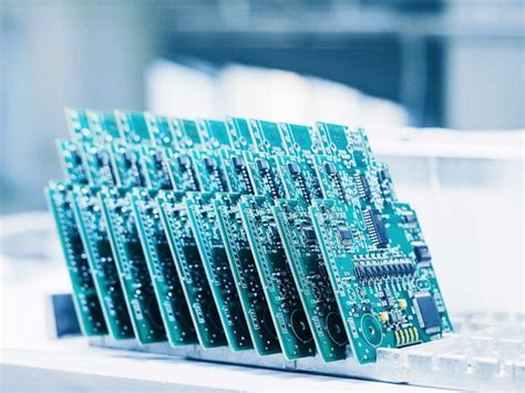
Cutting-Edge Materials in Modern PCB Assembly
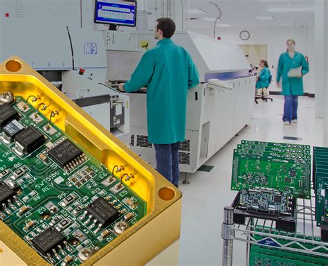
The landscape of PCB assembly is rapidly evolving, driven by the need for higher performance and reliability in today’s electronic devices. One of the most significant advancements lies in the development of cutting-edge materials that not only improve the durability of PCBA (Printed Circuit Board Assembly) but also enhance overall functionality. For instance, the incorporation of advanced substrates such as polyimide and ceramic materials offers superior thermal stability, making them ideal for high-temperature applications. Additionally, innovative conductive inks and coatings are revolutionizing the manufacturing process, enabling printed electronics that are lighter and more flexible compared to traditional copper-based boards. This flexibility facilitates new design possibilities, allowing engineers to create intricate circuits that were previously unattainable. Furthermore, these modern materials contribute to significant reductions in weight and size while maintaining electrical performance, which is crucial for mobile devices and wearable technologies. The integration of such advanced materials not only streamlines the PCB assembly process but also addresses environmental challenges by allowing for less waste through more efficient manufacturing techniques. As technologies continue to advance, staying at the forefront of material innovations will be essential for manufacturers aiming to meet the growing demands of modern electronics.
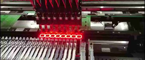
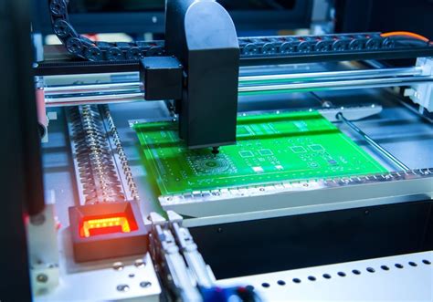
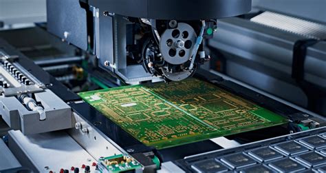
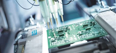
Automation and Robotics in PCB Production
The integration of automation and robotics in PCB assembly has revolutionized the manufacturing processes, driving significant improvements in precision and speed. With the adoption of advanced robotic systems, manufacturers can now achieve higher levels of consistency and accuracy in the placement of components on printed circuit boards. This advancement not only reduces the likelihood of human error but also enhances the overall quality of the printed circuit board assemblies (PCBA). The automation of repetitive tasks allows for increased productivity, enabling companies to meet growing market demands while minimizing waste. Furthermore, with cutting-edge technologies such as machine vision systems, robots can accurately inspect solder joints and component placement, ensuring that each unit meets stringent quality standards before leaving the production line. As a result, this shift toward automated PCB production is paving the way for more efficient workflows and has become essential for businesses striving to innovate. This ongoing evolution signifies a pivotal transformation in how modern electronics are manufactured, ultimately leading to more reliable and cost-effective consumer products.
Enhancing Efficiency through Advanced Processes
The landscape of PCB assembly has undergone remarkable transformation in recent years, leading to unprecedented levels of efficiency and reliability in electronic manufacturing. One significant advancement is the adoption of advanced processes such as selective soldering and automated optical inspection (AOI). These techniques not only streamline the PCBA workflow but also minimize human error, allowing for more precise soldering and component placement. Additionally, the integration of real-time data analytics has enabled manufacturers to monitor production processes closely, facilitating immediate adjustments that enhance yield rates and reduce waste. As a result, companies can achieve higher throughput without compromising the quality of the finished product. Moreover, modular assembly processes are being embraced, enabling manufacturers to quickly adapt to design changes or customer demands while maintaining operational efficiency. As these innovative practices continue to evolve, they promise to reshape the future of PCB manufacturing, proving crucial for meeting the ever-increasing demands of modern electronics while ensuring optimal performance and durability.
Sustainable Practices in PCB Manufacturing
The growing emphasis on environmental responsibility has prompted significant innovations in sustainable practices within PCB manufacturing and assembly. With the increasing demand for eco-friendly solutions, manufacturers are adopting new strategies to minimize waste and enhance resource efficiency. One notable approach is the use of lead-free solder and alternative materials that reduce the environmental impact of PCBA processes. Additionally, companies are implementing closed-loop systems, which recycle materials throughout manufacturing to decrease reliance on virgin resources. By optimizing energy consumption during the PCB assembly phase, manufacturers are not only cutting costs but also reducing their carbon footprint. Furthermore, advancements in smart manufacturing practices, such as utilizing IoT technology for real-time monitoring of production efficiency, allow for quicker identification of inefficiencies and waste. As a result, these sustainable practices not only benefit the environment but also enhance the overall quality and reliability of modern electronics, paving the way for a greener future in electronic circuit design.
Innovations in Circuit Design for Enhanced Performance
As the demand for more sophisticated electronics continues to surge, innovations in circuit design play a pivotal role in enhancing overall performance. Modern electronics require PCB assembly that not only integrates multiple functions but also optimizes space and reduces weight. One notable advancement is the shift towards high-frequency circuit design, allowing circuits to perform efficiently even at elevated frequencies, which is crucial for devices such as smartphones and wireless communication systems. Additionally, the adoption of new design methodologies, including multilayer PCBs and embedded components, has led to a significant increase in design density without compromising reliability.
Moreover, the integration of Internet of Things (IoT) capabilities has necessitated designs that support advanced connectivity. This evolution drives the necessity for enhanced routing techniques and improved signal integrity, which ultimately contribute to lower power consumption and increased performance longevity. The role of software tools for simulation and testing is also becoming increasingly important; such tools enable designers to predict performance issues and resolve them early in the design process, thus expediting time-to-market.
Furthermore, with the rise of automation in PCB manufacturing, innovative circuit designs can be seamlessly moved into production through advanced PCBA processes that leverage robotics and AI technologies. This synergy between circuit design innovations and effective assembly techniques ensures that modern electronic devices meet consumer expectations for speed, reliability, and efficiency while remaining environmentally sustainable. As these trends continue to evolve, we can anticipate even more groundbreaking changes that will shape the future landscape of electronics.
The Role of AI and Machine Learning in PCB Development
The integration of AI and Machine Learning into PCB assembly processes is transforming the landscape of circuit development. These technologies allow manufacturers to analyze vast amounts of data quickly, enhancing decision-making and identifying potential issues before they arise. By utilizing advanced algorithms, organizations can optimize every stage of the pcba process, from layout design to final assembly. For instance, predictive maintenance powered by machine learning algorithms can significantly reduce downtime by anticipating failures in manufacturing equipment. Moreover, AI-driven tools facilitate improved quality control by examining components and assemblies with unprecedented precision, thus minimizing defects. This ensures that PCBs maintain their integrity and reliability in various applications, reflecting a higher standard of performance expected in modern electronics. Furthermore, the capability of machine learning to self-improve through continuous data input means that PCB manufacturing can become more adaptive, allowing for rapid adjustments based on market demands or technological advancements. As these tools become more prevalent, they are expected to redefine the future standards for efficiency and accuracy in the PCB assembly sector.
Future Trends in PCB Technologies and Applications
As the demand for more complex and compact electronic devices grows, the pcb assembly industry is witnessing several transformative trends. One major trend is the increased adoption of flexible printed circuit boards (FPCBs), which offer unparalleled adaptability in design while reducing overall weight. These advancements allow for innovative applications in sectors such as wearable technology and mobile devices. Additionally, microvia technology has gained prominence, facilitating the creation of high-density interconnections that can significantly enhance performance while minimizing footprint size. Another notable trend is the integration of smart manufacturing techniques within pcba processes; leveraging automation, data analytics, and IoT connectivity not only optimizes production efficiency but also enhances quality control measures. Furthermore, as sustainability becomes a pivotal concern in electronics manufacturing, innovations such as lead-free soldering and recycling programs for electronic waste are emerging as vital components of future pcb technologies. Together, these advancements are paving the way for smarter designs that not only meet the performance demands of modern applications but also adhere to environmental standards.
Conclusion
In summary, the landscape of PCB manufacturing and assembly (often referred to as PCBA) is rapidly transforming through a combination of innovative practices and cutting-edge technologies. As the demand for more compact and efficient electronics escalates, advancements such as enhanced material compositions and complex manufacturing techniques are playing a pivotal role. Emerging trends emphasize the integration of automation and robotics to streamline production processes, significantly reducing lead times while improving overall product quality. Furthermore, the impact of sustainable practices cannot be overstated, as manufacturers strive for eco-friendly solutions without compromising performance. The ongoing evolution in circuit design also offers exciting possibilities for enhanced functionality in modern devices. Ultimately, these developments not only ensure enhanced reliability in pcb assemblies but also pave the way for future trends that will significantly shape the trajectory of electronics design and production. As we look ahead, it is evident that embracing these innovations will be crucial for both manufacturers and consumers seeking to thrive in a competitive market defined by rapid technological advancements.
FAQs
What is PCB assembly (PCBA)?
PCB assembly, often referred to as PCBA, is the process of connecting electronic components to a printed circuit board (PCB). This involves soldering components onto the board to create a functional electronic circuit that powers various devices.
What advancements are currently influencing PCB assembly?
Recent innovations in PCB assembly include advanced materials that improve thermal efficiency and reliability, as well as automated processes that enhance production speed and reduce errors. Technologies such as robotics and precision machinery are playing a crucial role in these advancements.
How do automation and robotics improve PCB manufacturing?
Automation and robotics streamline the PCB manufacturing process by reducing manual labor, increasing precision, and minimizing production time. Machines can perform repetitive tasks more efficiently than humans, leading to higher output quality in PCBA.
What sustainable practices are being implemented in PCB manufacturing?
Sustainable practices in PCB manufacturing focus on using environmentally friendly materials, reducing waste during production, and recycling components whenever possible. These approaches aim to lower the overall environmental impact of electronics manufacturing.
How do innovations in circuit design affect PCBA?
Innovations in circuit design lead to more efficient layouts and enhanced functionality. By optimizing designs for smaller spaces, manufacturers can produce lighter and more compact electronic devices while maintaining or improving performance.
For more information about advanced PCB assembly, please visit this link for comprehensive insights into current trends and technologies that are shaping the future of electronics.