Innovations in Printed Circuit Board Assembly and Design Solutions
Key Takeaways
In the fast-evolving realm of pcb assembly and design solutions, several key factors are influencing both efficiency and performance in electronic manufacturing. Firstly, the continuous advancement in materials used for pcba is crucial. Innovations such as flexible substrates and high-density interconnects enable the creation of more compact and reliable electronic devices. Additionally, sophisticated techniques in pcb assembly, such as surface mount technology (SMT) and automated soldering methods, have significantly improved production speed while maintaining quality standards.
Another noteworthy aspect is the impact of automation in modern pcb assembly processes. With the integration of robotics and artificial intelligence, manufacturers can achieve higher precision in placing components and reduce human error. This not only enhances productivity but also lowers operational costs.
To further streamline the manufacturing process, advancements in pcb design software play a vital role. Such tools facilitate comprehensive simulations and design tests that anticipate issues before production begins, thus minimizing waste and rework.
As sustainability becomes increasingly important, greener practices are also finding their way into pcba methodologies. Utilizing recyclable materials and adopting energy-efficient processes not only benefits the environment but can also lead to regulatory compliance advantages.
Here’s a summary table to illustrate these key advancements:
| Area | Innovation |
|---|---|
| Materials | Flexible substrates, high-density interconnects |
| Techniques | Surface mount technology (SMT), automated soldering |
| Automation | Robotics integration for precision |
| Software | Advanced PCB design tools for simulation |
| Sustainability Practices | Use of recyclable materials, energy-efficient processes |
In conclusion, understanding these advancements will prepare stakeholders for upcoming challenges while keeping them at the forefront of printed circuit board assembly technology.
The Evolution of Printed Circuit Board Assembly: A Historical Perspective
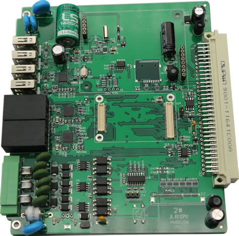
The journey of pcb assembly has been transformative, reflecting advancements in technology and changes in consumer demands. Initially, printed circuit boards (PCBs) were manually assembled, often leading to inconsistencies and limitations in design. However, the introduction of automated pcba processes revolutionized this industry. By reducing human error and improving production efficiency, automation has enabled manufacturers to produce high volumes of pcba with greater precision.
Moreover, the development of multilayered PCBs has expanded the possibilities for electronic designs, allowing for more complex circuitry in compact formats. As materials science progressed, innovations such as high-frequency laminates and lead-free soldering technologies emerged, enhancing the performance and reliability of pcb assembly products.
As we reflect on this evolution, it is clear that collaboration among engineers, designers, and manufacturers has played a crucial role in driving these developments forward.
“Innovation is the key driver in maintaining a competitive edge within the electronic manufacturing realm.”
Through ongoing advancements in design solutions and assembly techniques, the future looks promising for pcb assembly, suggesting continued improvements in efficiency and sustainability that will shape the landscape of electronics manufacturing for years to come.
Emerging Materials in Printed Circuit Board Design
In the rapidly evolving world of printed circuit board assembly (PCB assembly), the introduction of innovative materials is paramount to enhancing performance and reliability. The shift towards lightweight yet durable materials is driven by the increasing demand for higher functionality in PCBA applications. For instance, materials such as flexible substrates and high-frequency laminates are emerging as game-changers, offering superior electrical performance and reduced size. Furthermore, the incorporation of conductive inks—which allow for printed circuitry directly on flexible surfaces—has opened new avenues for design freedom and manufacturing efficiency. These advancements not only allow for more compact designs but also contribute to improved thermal management, which is crucial for high-performance electronics. The combination of these emerging materials with advanced fabrication technologies enables designers to create PCBA solutions that meet the complex requirements of modern electronic devices while maintaining a cost-effective production process. As these materials continue to evolve, they are set to redefine standards in reliability and sustainability, paving the way for future innovations in PCB design and assembly practices.
Advanced Techniques in PCB Assembly for Enhanced Performance
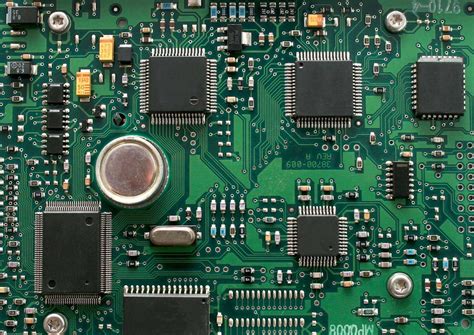
In the realm of PCB assembly (PCBA), a variety of advanced techniques have emerged that significantly improve performance and efficiency in electronic manufacturing. One such technique involves the utilization of automated optical inspection (AOI), which allows for the rapid identification of defects during the assembly process. This automation not only speeds up production times but also enhances overall reliability by ensuring that only boards meeting stringent quality criteria proceed to further stages of manufacturing.
Additionally, the integration of micro-vias and buried vias in printed circuit boards allows for a more compact design, reducing space while increasing the connectivity options available for various electronic components. This miniaturization enables manufacturers to create denser boards without sacrificing performance, making it particularly beneficial in industries where size constraints are critical, such as mobile devices and wearable technology.
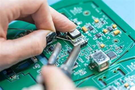
Moreover, advancements in soldering techniques, such as selective soldering, provide enhanced control over heat application. This method minimizes thermal exposure to sensitive components, thereby improving their longevity and performance. The use of lead-free solders is also becoming increasingly popular due to environmental regulations, and these innovations ensure that manufacturers can produce high-quality assemblies while adhering to sustainability goals.
In conclusion, these advanced techniques in PCB assembly, including automated inspection, micro-vias, and state-of-the-art soldering, are transforming the landscape of electronic manufacturing by enhancing performance metrics significantly. The continued evolution of these methods will undoubtedly pave the way for even greater innovations in PCBA efficiencies and capabilities.
The Role of Automation in Modern PCB Manufacturing
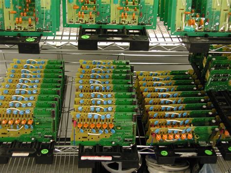
The introduction of automation in PCB assembly has significantly transformed the landscape of electronic manufacturing. Through the use of advanced robotics and intelligent systems, pcba processes are now characterized by enhanced precision and reduced human error. Automation facilitates faster production cycles, allowing manufacturers to meet increasing demand without sacrificing quality. Furthermore, the integration of automated inspection systems ensures that any defects are identified early in the production process, ultimately leading to higher reliability in the end product. In addition to improving efficiency, automation also allows for flexible scalability; manufacturers can quickly adjust their operations in response to changing market requirements or specific customer needs. This adaptability is crucial in a fast-paced industry where innovation and speed are paramount. The synergistic combination of automation with emerging technologies such as artificial intelligence and machine learning is paving the way for even more groundbreaking advancements in pcb assembly practices, fostering a new era of smarter manufacturing solutions that promise not only efficiency but also enhanced performance and sustainability. As these technologies continue to evolve, so does the potential for pcba processes to revolutionize how electronic components are designed and assembled, ensuring ongoing progress within this vital sector.
Innovations in PCB Design Software: Streamlining the Process
The rapid evolution of PCB design software has played a pivotal role in transforming pcb assembly processes, making them more efficient and reliable. With the introduction of advanced computational tools, designers can now simulate electronic circuits and PCB layouts in real time. This newfound capability enables the identification of potential issues before physical prototypes are created, significantly reducing the time and costs associated with traditional prototyping. Furthermore, these innovative software solutions support pcba verification through integrated testing features, ensuring a seamless transition from design to manufacturing. Enhanced collaboration tools within these platforms facilitate teamwork among engineers and designers across different geographical locations, promoting an integrated approach to development. As a result, companies can swiftly adapt to market demands and customize their pcb assembly solutions to meet specific client needs while maintaining high standards of quality and performance. In summary, advancements in PCB design software not only streamline the overall process but also enhance the possibilities for developing groundbreaking electronic products.
Sustainability in Printed Circuit Board Assembly Practices
The drive towards sustainability in pcb assembly practices is becoming increasingly significant as the electronics industry aims to reduce its environmental footprint. Sustainability in pcba not only involves the use of eco-friendly materials but also encompasses efficient manufacturing processes that conserve energy and minimize waste. Manufacturers are adopting innovative techniques such as lead-free soldering and the utilization of recyclable materials, which contribute to reducing harmful emissions and chemicals associated with traditional methods. Moreover, advancements in technology allow for finer and more precise designs, which result in more efficient usage of materials. Companies are now prioritizing circular economy principles by implementing take-back programs that ensure old circuit boards are properly recycled or refurbished instead of ending up in landfills. With the integration of green technologies and practices, pcb assembly is evolving to meet both industry demands and environmental responsibilities, paving the way for a more sustainable future.
Future Trends in PCB Technology and Market Implications
As we look ahead in the world of pcb assembly, several key trends are emerging that promise to reshape the landscape of electronic manufacturing. One prominent trend is the increasing adoption of automation within pcba processes. By integrating advanced robotics and machine learning technologies, manufacturers are not only enhancing the speed of assembly but also significantly increasing precision, ultimately resulting in superior product quality. Furthermore, innovations in materials science are contributing to the development of more efficient printed circuit boards, while simultaneously addressing sustainability concerns. For instance, eco-friendly materials are being utilized to reduce environmental impact without compromising performance.
Another essential trend is the integration of IoT (Internet of Things) technologies into pcb assembly workflows, allowing for real-time monitoring and data analysis. This interconnectedness enables manufacturers to make informed decisions on optimizing production processes and achieving greater operational efficiencies. Additionally, as devices become increasingly compact and complex, there is a rising demand for sophisticated design solutions that can support denser component layouts without sacrificing reliability.
Finally, collaboration between software developers and hardware manufacturers has led to significant advancements in PCB design software, simplifying the design process through clearer interfaces and enhanced functionalities. These innovations allow engineers to rapidly prototype new solutions, adapting more swiftly to market demands while ensuring that their products remain competitive. In summary, these future trends in pcb technology not only highlight a shift towards automation and eco-consciousness but also underscore a commitment to innovation that will be crucial as the industry navigates ongoing challenges and opportunities.
Case Studies: Successful Implementations of Innovative PCB Solutions
In recent years, the landscape of pcb assembly has undergone remarkable transformations, fueled by advancements in technology and materials. Several case studies illustrate how companies are successfully integrating innovative techniques into their pcba processes, significantly enhancing efficiency and performance. One notable example involves a leading electronics manufacturer that adopted a new automated soldering technique that reduced assembly time by over 30%. This advancement not only optimized production schedules but also led to a noticeable decrease in defects, ultimately improving product quality. Another case highlights the use of advanced flexible materials in the design of circuit boards. By incorporating these materials, the company was able to create slimmer and more adaptable products that cater to the growing demand for space-saving technology in consumer electronics. These case studies underscore the critical role that innovative pcb assembly practices play in driving success within the industry, showcasing how effective implementation of cutting-edge solutions can lead to significant competitive advantages and meet evolving market needs. As manufacturers continue to embrace new technologies and design principles, the potential for further advancements in pcb assembly will remain strong, paving the way for even more transformative outcomes in electronic manufacturing.
Conclusion
In summary, the world of PCB assembly has witnessed remarkable transformations driven by the incorporation of advanced technologies and innovative materials. This ongoing evolution not only enhances the efficiency of PCBA processes but also significantly improves performance outcomes in electronic manufacturing. Recent advances such as automated assembly techniques and sophisticated design software facilitate a smoother and more precise approach to printed circuit board manufacturing. Moreover, the emergence of sustainable practices within pcb assembly underscores a commitment to environmentally friendly solutions that meet both regulatory standards and market demands. As industries continue to explore future trends, there is a clear indication that printed circuit board assembly will increasingly prioritize adaptability and innovation, paving the way for more reliable and high-performing electronic products in various applications.
FAQs
What is PCB assembly?
PCB assembly, often abbreviated as PCBA, is the process of soldering electronic components onto a printed circuit board (PCB) to create a functional electronic device. This process includes various techniques such as surface mount technology (SMT) and through-hole technology.
What materials are commonly used in PCB assembly?
In PCB assembly, the materials include high-quality substrates like FR-4, copper for conducting pathways, and various solder types that ensure strong connections between components and the PCB. Advanced options may incorporate innovative materials that enhance thermal and electrical performance.
How does automation impact PCB assembly?
Automation has revolutionized pcb assembly processes by increasing efficiency and accuracy. Automated machines can solder components with precision, reducing the likelihood of human error and accelerating production timelines.
What are some advanced techniques in PCBA?
Advanced techniques in PCBA encompass methods like selective soldering, robotic pick-and-place systems, and inspection technologies such as Automated Optical Inspection (AOI). These innovations significantly enhance the quality and reliability of electronic assemblies.
Why is sustainability important in PCB assembly?
Sustainability in pcb assembly addresses environmental concerns by promoting practices that reduce waste and energy consumption. Utilizing eco-friendly materials and processes not only benefits the planet but also meets growing regulatory standards.


