Innovative PCB Design Strategies for Next-Generation Electronics

Key Takeaways
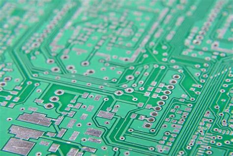
Effective PCB design for next-generation electronics hinges on balancing high-density layouts, thermal management, and signal integrity. Leading manufacturers leverage advanced HDI (High-Density Interconnect) techniques to accommodate complex circuitry in compact spaces, ensuring optimal performance for PCBA applications. Innovations like embedded components and stacked microvias are critical for minimizing signal loss in high-speed designs.
Tip: Always prioritize design for manufacturability (DFM) during layout planning to avoid costly rework during PCB assembly.
Thermal challenges in modern electronics demand strategic placement of thermal vias and advanced materials like metal-core substrates to dissipate heat efficiently. Simultaneously, maintaining signal integrity requires meticulous trace routing, impedance matching, and the use of low-loss dielectric materials. For PCBA workflows, integrating simulation tools early in the design phase helps identify potential electromagnetic interference (EMI) risks.
Emerging technologies such as flex-rigid PCBs and 3D-printed circuitry are reshaping design paradigms, enabling lighter and more durable solutions. By adopting these strategies, PCB designing companies can deliver robust, scalable designs that meet the demands of 5G, IoT, and AI-driven systems.

Advancing PCB Design for Future Electronics
As next-generation electronics demand higher performance in compact form factors, PCB designing companies are redefining their methodologies to address evolving challenges. Central to this evolution is the integration of high-density interconnect (HDI) technologies, enabling complex circuitry within shrinking board dimensions. Engineers now leverage advanced software tools to optimize layer stacking and microvia placement, ensuring seamless pcb assembly workflows while minimizing signal loss.
A critical focus lies in balancing thermal efficiency with electrical performance. Modern designs incorporate thermally conductive substrates and strategic copper pours to dissipate heat effectively, especially in high-power applications like 5G modules or AI processors. For instance, the table below highlights key thermal management strategies:
| Strategy | Application | Impact |
|---|---|---|
| Embedded heat sinks | High-power ICs | 20-30% thermal reduction |
| Thermal vias | Multilayer boards | Improved heat distribution |
| Ceramic-filled substrates | Automotive electronics | Enhanced reliability |
Signal integrity remains paramount, particularly for PCBA-driven systems requiring ultrafast data transfer. Techniques like differential pair routing and impedance matching are now augmented with AI-driven simulation tools to predict EMI/ESD risks pre-production. Additionally, the shift toward flex-rigid hybrid boards supports innovative form factors in wearables and IoT devices.
To address these complexities, leading firms are adopting collaborative frameworks, as detailed in this resource on PCB layout challenges. By merging interdisciplinary expertise with cutting-edge pcb assembly processes, the industry is poised to deliver electronics that are not only smaller and faster but also more resilient to operational stresses.
High-Density PCB Layout Optimization Techniques
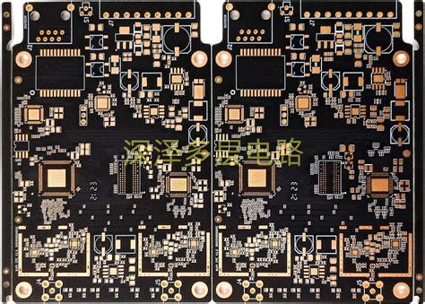
Achieving optimal performance in next-generation electronics demands precision in high-density PCB layout design. As components shrink and functionality expands, engineers must balance space constraints with electrical efficiency. A critical focus lies in minimizing parasitic capacitance and inductance through strategic trace routing, such as employing differential pairs for high-speed signals and avoiding parallel runs that induce crosstalk. Advanced pcb assembly workflows now integrate HDI (High-Density Interconnect) technologies, leveraging microvias and stacked copper layers to reduce board footprint while enhancing signal pathways.
Thermal management is inherently tied to layout decisions—placing high-power components near thermal vias or heatsinks prevents localized overheating. Simulation tools like 3D electromagnetic field solvers enable designers to predict and mitigate hotspots before PCBA testing phases. Additionally, optimizing pad geometries and solder mask apertures ensures reliable connections during pcb assembly, particularly for fine-pitch components like BGAs or QFNs.
Collaboration between layout engineers and pcb assembly partners, such as MicroArt Services, streamlines design-for-manufacturability (DFM) checks. This alignment reduces rework risks by addressing annular ring tolerances and via-in-pad specifications early. By integrating signal integrity analysis into the layout phase, PCB designing companies can preemptively resolve impedance mismatches, ensuring robust performance in high-frequency applications like 5G or IoT devices.

Thermal Management in Modern PCB Engineering
Effective thermal management has become a cornerstone of high-performance electronics, particularly as PCB designing companies push the limits of miniaturization and power density. Modern designs integrate advanced techniques like embedded heat sinks, thermally conductive vias, and copper pours to dissipate heat efficiently. For PCBA (printed circuit board assembly) processes, material selection plays a critical role—high-temperature laminates and low-thermal-resistance substrates ensure stability under operational stress.
Innovative approaches such as dynamic thermal simulation allow engineers to predict hotspots during PCB assembly, optimizing component placement and trace routing. Leading firms also leverage active cooling systems, including microfluidic channels or piezoelectric fans, to complement passive solutions. These strategies are vital for applications like 5G infrastructure and AI-driven devices, where sustained performance relies on preventing thermal throttling.
Collaboration between PCB designing companies and thermal simulation specialists ensures designs meet both electrical and thermal requirements. This synergy is particularly evident in multi-layer PCBA configurations, where balancing signal integrity with heat dissipation demands precision. As next-gen electronics demand faster processing in compact form factors, mastering thermal management remains a defining challenge for the industry.
Signal Integrity Solutions for Next-Gen PCBs
Maintaining signal integrity in next-generation electronics demands precision-driven strategies, particularly as devices evolve toward higher frequencies and denser architectures. Leading PCB designing companies employ advanced simulation tools to model electromagnetic interference (EMI), crosstalk, and impedance mismatches early in the design phase. By integrating high-speed routing protocols like differential pair routing and controlled impedance traces, engineers minimize signal distortion across high-density interconnects (HDIs).
A critical focus lies in optimizing stack-up configurations to balance signal layers with ground planes, reducing parasitic capacitance and inductive coupling. For instance, using low-loss dielectric materials such as Rogers or Isola substrates enhances signal propagation in 5G and IoT applications. Additionally, pcb assembly processes are refined through automated optical inspection (AOI) and 3D X-ray verification to ensure precise alignment of microvias and buried traces, which directly impacts signal performance.
Collaboration between design and pcba teams is vital for addressing post-production challenges. Real-time testing with vector network analyzers (VNAs) validates signal paths, while added-value services like signal integrity audits provide actionable insights for iterative improvements. By adopting these methodologies, manufacturers achieve robust signal-to-noise ratios (SNRs) even in ultra-compact, multi-board systems, paving the way for reliable high-frequency electronics.
Cutting-Edge Strategies in PCB Design Innovation
To meet the demands of next-generation electronics, PCB designing companies are adopting revolutionary methodologies that blend precision engineering with advanced computational tools. One standout approach involves leveraging AI-driven topology optimization to balance high-density interconnect (HDI) layouts with thermal and electrical performance. By integrating 3D-printed circuitry and embedded passive components, designers achieve unprecedented space efficiency while reducing parasitic effects.
Another critical strategy focuses on thermal management through microvia-in-pad technologies and advanced material stacks, such as thermally conductive substrates. These innovations are particularly vital for pcb assembly processes, where heat dissipation directly impacts PCBA reliability in compact devices like wearables and IoT modules.
Additionally, the use of machine learning algorithms to predict signal integrity issues during early design phases is reshaping validation workflows. Forward-thinking firms now simulate electromagnetic interference (EMI) scenarios across multi-layered boards, ensuring compliance with high-frequency standards. Collaboration between PCB designing companies and PCBA manufacturers further streamlines prototyping, enabling rapid iteration of mixed-signal designs for 5G and AI-driven applications.
By merging modular design philosophies with scalable fabrication techniques, the industry is poised to deliver electronics that are not only smaller and faster but also inherently adaptable to evolving technological landscapes.
PCB Designing Companies’ Expert Approaches
Leading PCB designing companies leverage multidisciplinary expertise to address the complexities of modern electronics. By integrating PCB assembly (PCBA) considerations early in the design phase, these firms ensure seamless transitions from schematic concepts to functional prototypes. Their methodologies often combine automated routing algorithms with manual fine-tuning, balancing high-density layouts with manufacturability constraints. For instance, advanced thermal simulation tools enable precise heat dissipation planning, while impedance-matching strategies maintain signal integrity in high-frequency applications.
A hallmark of expert approaches is the use of HDI (High-Density Interconnect) technologies, which optimize space utilization without compromising reliability. Collaborations with PCBA partners further enhance design validation, as real-world testing identifies potential bottlenecks in solder joint integrity or component placement. Additionally, progressive firms adopt AI-driven design assistants to predict electromagnetic interference patterns, reducing iteration cycles.
To support next-generation requirements, many companies now prioritize material innovation, employing low-loss substrates and flexible laminates. This aligns with industry shifts toward miniaturized, IoT-enabled devices. By embedding PCB assembly insights into initial design frameworks, these experts ensure scalability across production phases, from prototyping to mass PCBA manufacturing. Such holistic strategies underscore their role in pushing the boundaries of electronic performance while maintaining rigorous quality benchmarks.

Next-Generation Electronics: PCB Design Breakthroughs
Leading PCB designing companies are redefining electronics manufacturing through innovations that address the growing demands of miniaturization and performance. By leveraging advanced materials like high-density interconnect (HDI) substrates and flexible laminates, engineers achieve high-density layouts without compromising reliability. These breakthroughs enable tighter component placement, critical for wearables and IoT devices where space constraints dominate.
A key advancement lies in integrating thermal management solutions directly into PCBA workflows. Techniques such as stacked microvias and embedded heat-dissipating materials mitigate overheating risks in compact designs. Simultaneously, signal integrity is preserved through precision-controlled impedance matching and advanced simulation tools, ensuring stable performance in high-frequency applications like 5G infrastructure.
The shift toward modular PCB assembly processes further enhances scalability. By adopting automated optical inspection (AOI) and AI-driven defect detection, PCB designing companies reduce time-to-market while maintaining stringent quality standards. These strategies not only optimize PCBA workflows but also pave the way for sustainable practices, such as recyclable substrate usage and energy-efficient manufacturing.
As next-gen electronics push boundaries, collaboration between design and production teams remains pivotal. Innovations in multi-physics simulation and hybrid rigid-flex designs underscore the industry’s commitment to balancing complexity with functionality, solidifying PCB assembly as the backbone of modern electronics evolution.
Optimizing PCB Performance in Advanced Electronics
Achieving peak performance in advanced electronics demands meticulous attention to PCB assembly processes and material selection. Leading PCB designing companies leverage high-density interconnect (HDI) substrates to minimize signal loss while accommodating complex circuitry. By integrating PCBA-specific design rules, such as controlled impedance routing and via-in-pad techniques, engineers enhance signal integrity in high-frequency applications. Thermal management remains critical; advanced embedded cooling solutions and thermally conductive substrates are now standard in designs targeting high-power components like GPUs and AI accelerators.
To address electromagnetic interference (EMI), designers employ shielding techniques such as grounded copper pours and strategic layer stacking. For example, automated test equipment (ATE) boards often utilize multi-layered designs with dedicated power planes to isolate sensitive analog and digital sections. Additionally, design-for-manufacturability (DFM) principles ensure seamless transitions from prototyping to mass production, reducing defects during PCB assembly. Real-time simulation tools further validate thermal and electrical performance, enabling iterative optimization before fabrication.
As next-gen electronics push miniaturization limits, PCBA workflows increasingly rely on advanced solder mask technologies and microvia drilling to maintain reliability in ultra-compact layouts. These strategies, paired with rigorous testing protocols, position modern PCB designing companies to deliver robust solutions for 5G, IoT, and automotive systems.
Conclusion
As the electronics industry evolves, PCB designing companies must balance innovation with practical implementation to meet escalating demands. The integration of advanced techniques—from high-density interconnects to adaptive thermal management—ensures that next-generation devices achieve both compactness and reliability. By leveraging pcb assembly expertise, engineers can translate complex designs into functional hardware, while pcba processes refine manufacturability without compromising performance.
Successful strategies hinge on collaboration between design and manufacturing teams, ensuring signal integrity and power distribution remain optimal across prototyping and mass production. Emerging tools like AI-driven simulation further enable rapid iteration, reducing time-to-market for cutting-edge electronics.
Ultimately, the future of PCB design lies in harmonizing novel methodologies with proven practices. As pcb designing companies adopt hybrid approaches—combining modular architectures with sustainable materials—they pave the way for scalable, future-proof solutions. This synergy between creativity and technical rigor will define the next era of electronic innovation, where functionality and efficiency coexist seamlessly.
Frequently Asked Questions
How do PCB assembly processes impact design complexity in next-gen electronics?
Advanced PCBA requires precise coordination between layout engineers and manufacturing teams. Designers must account for component placement density and thermal dissipation paths to ensure compatibility with automated assembly lines, particularly for high-density interconnect (HDI) boards.
What strategies ensure optimal thermal management in compact PCB designs?
Leading firms employ embedded cooling channels and thermal vias alongside PCB assembly protocols that prioritize heat-resistant materials. Simulations using computational fluid dynamics (CFD) help validate thermal performance before prototyping.
Why is signal integrity critical for high-speed PCB applications?
With 5G and IoT devices demanding faster data rates, PCBA specialists utilize impedance-controlled routing and ground plane optimization to minimize electromagnetic interference (EMI). Advanced signal integrity analysis tools are now integrated into design workflows.
How are PCB designing companies adapting to evolving industry standards?
Top-tier providers implement AI-driven design validation and flex-rigid hybrid boards to meet IPC-6012 Class 3 specifications. Collaboration with PCB assembly partners during the design-for-manufacturing (DFM) phase ensures compliance with automotive and aerospace reliability requirements.
Ready to Optimize Your Next PCB Project?
For tailored PCB assembly solutions that align with cutting-edge design strategies, please click here to consult our engineering team.