Innovative Techniques in Double Layer PCB Manufacturing
Key Takeaways
In the evolving field of pcb manufacturing, it is essential to grasp the key takeaways to stay ahead in this competitive landscape. One of the primary considerations is the pcb manufacturing cost, which can significantly affect your overall production budget. By choosing innovative materials, you can not only enhance performance but also optimize costs in your pcb manufacturing business. Additionally, staying informed about advancements in pcb manufacturing companies allows you to leverage cutting-edge technologies that improve both speed and efficiency in production processes.
The integration of streamlined processes and quality assurance testings ensures that your double-layer PCBs meet high performance standards, thus attracting customers looking for reliability and durability in their electronic components. Understanding the latest trends and case studies from leaders in the industry can further prepare you for future developments. Engaging with resources such as Andwin PCB offers valuable insights into successful implementations and innovative practices within double-layer PCB technology.
By focusing on these crucial aspects, you can position your pcb manufacturing business for ongoing success and adaptability in an ever-changing market landscape.
Introduction to Double Layer PCB Manufacturing
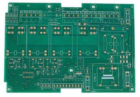
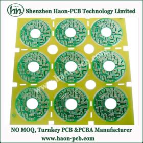
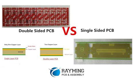
When you delve into double layer PCB manufacturing, it’s essential to grasp the core of what sets this technique apart from others. These PCBs, or printed circuit boards, are pivotal in your electronic devices, enabling efficient connectivity and functionality. The pcb manufacturing process for double layer boards involves a meticulous arrangement of layers that optimizes the pathways for electricity while minimizing overall space and weight. As you navigate through the landscape of pcb manufacturing companies, you’ll notice a strong emphasis on innovation, particularly in the realms of design and materials. The integration of advanced technologies not only lowers the pcb manufacturing cost but also enhances durability and performance, making your devices more reliable over time.
Moreover, these manufacturers are increasingly focusing on sustainability practices within their pcb manufacturing business, incorporating eco-friendly materials and processes that align with global environmental standards. As you explore these advancements, consider how they directly impact your projects—potentially reducing costs while improving functionality. Understanding these innovations gives you a valuable perspective on how to select the best products and partners in the ever-evolving field of electronics manufacturing.
Key Advancements in PCB Design Techniques
In the evolving landscape of PCB manufacturing, significant advancements in design techniques are reshaping how professionals approach the development of double layer PCBs. One of the fundamental changes is the integration of computer-aided design (CAD) tools that enhance precision and speed in layout creation. These tools allow you to visualize and optimize circuits, ensuring effective space utilization while minimizing interference and signal degradation. Moreover, utilizing advanced simulation software empowers you to test performance outcomes before physical prototypes are produced, thus reducing the PCB manufacturing cost significantly.
Another notable advancement is the implementation of high-frequency design techniques. As modern electronics demand faster data transfer rates, optimizing trace width and spacing becomes critical. Embracing these techniques not only aids in achieving better performance but also supports your venture if you’re part of a PCB manufacturing business that caters to high-tech sectors. Additionally, developments in design for manufacturability (DFM) principles encourage early consideration of manufacturing processes in the design phase, which inevitably leads to a reduction in errors during production.
“Harnessing innovative design techniques not only elevates product performance but also provides a competitive edge within the industry.”
As you explore these advancements, collaborating with forward-thinking PCB manufacturing companies can offer insights into how these innovations are applied practically. By staying abreast of current trends and integrating modern practices into your operations, you enhance your capacity to deliver high-quality products that meet market demands efficiently and effectively. Thus, understanding these key advancements is vital for anyone involved in double layer PCB production to remain at the forefront of technology and innovation.

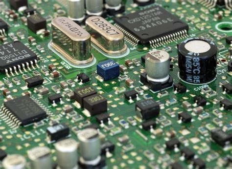
Innovative Materials Driving Performance Improvements
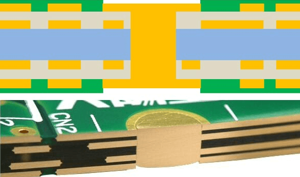
In the realm of double layer PCB manufacturing, innovative materials are key to enhancing overall performance and reliability. You may find that newly developed substrates offer superior thermal management, allowing for higher power densities while minimizing the risk of overheating. These advancements not only contribute to improved functionality but also play a pivotal role in reducing the PCB manufacturing cost through increased efficiency. Furthermore, the integration of advanced materials such as flexible laminates and high-frequency RF materials is revolutionizing the way PCB manufacturing companies approach intricate designs. With better signal integrity and reduced losses, you can expect your projects to achieve longer lifespans and enhanced performance metrics. As you delve deeper into the PCB manufacturing business, it will become evident that the choice of materials significantly influences not just production costs but also end-product quality. Embracing these innovative materials not only streamlines your design process but also positions your business at the forefront of modern electronics development, ensuring you stay competitive in a rapidly evolving market landscape.
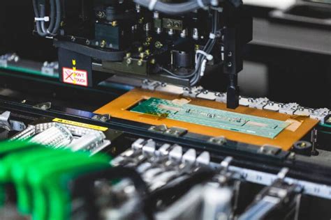
Streamlining Production Processes for Efficiency
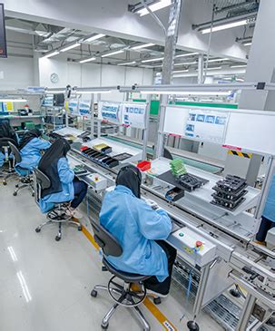
In today’s competitive landscape of pcb manufacturing, efficiency is more than a buzzword; it’s a necessity. To optimize operations, pcb manufacturing companies are increasingly adopting innovative strategies that significantly enhance productivity. One of the key methods is integrating advanced automation technologies into the production line. This not only reduces manual errors but also accelerates the manufacturing cycle, ultimately leading to lower pcb manufacturing cost. Additionally, lean manufacturing principles are being applied to minimize waste and optimize resource utilization. For you to remain competitive within the pcb manufacturing business, it’s crucial to focus on creating a streamlined workflow that fosters collaboration among different departments while leveraging real-time data analytics for decision-making. The shift towards a more digitized manufacturing process can make your operations not only faster but also more adaptable to market changes, ensuring you meet customer demands swiftly and efficiently. In essence, by prioritizing operational efficiency through innovative production processes, you position your business for sustained success in the dynamic industry of double layer PCB products.
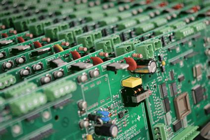
Testing and Quality Assurance in Double Layer PCBs
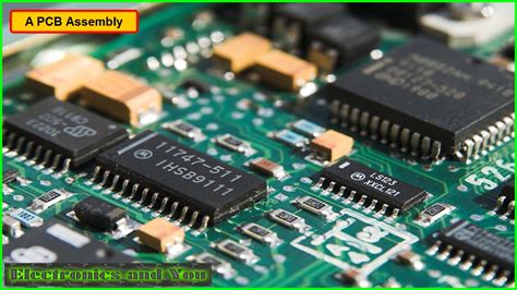
To ensure the reliability and performance of your double layer PCB manufacturing, implementing rigorous testing and quality assurance measures is essential. As a key player in the PCB manufacturing business, you understand that defects can lead to significant costs and setbacks in production. Thus, employing standardized testing protocols allows you to scrutinize various parameters of the PCB manufacturing process, including electrical conductivity, insulation resistance, and mechanical integrity.
Utilizing advanced technologies like automated optical inspection (AOI) can streamline your quality checks while reducing the overall PCB manufacturing cost. By adopting real-time monitoring during production, you can detect anomalies early, ensuring that your products meet both industry standards and customer expectations. Collaborating with reputable PCB manufacturing companies that prioritize quality can further enhance your confidence in the end product. As you focus on maintaining high-quality output, consider integrating these testing methodologies not just as a regulatory requirement but as a strategic advantage that differentiates your offerings in the competitive landscape of electronic assembly.
Future Trends in PCB Technology and Manufacturing
As you delve into the future trends in PCB technology and manufacturing, it becomes clear that ongoing innovations will shape the landscape of double layer PCB manufacturing. One of the most notable trends includes the integration of advanced software tools that aid in efficient PCB design, allowing you to tailor layouts for optimal performance. Moreover, with a focus on sustainability, pcb manufacturing companies are increasingly investing in eco-friendly materials that not only reduce the overall pcb manufacturing cost but also enhance product longevity. You will also observe an uptick in automation within production lines; this shift not only streamlines operations but dramatically reduces lead times, giving businesses a competitive edge in the burgeoning pcb manufacturing business sector. As manufacturers adopt cutting-edge techniques and tools, you can expect a marked improvement in both product efficiency and functionality, setting a new standard for what double layer PCBs can achieve. Embracing these advancements will be crucial for anyone looking to stay ahead in the rapidly evolving electronics industry.
Case Studies: Successful Implementations of Double Layer PCBs
You may find that the double layer PCB manufacturing landscape has evolved through various successful case studies that demonstrate the capabilities of modern technology and innovation. These implementations highlight how specific PCB manufacturing companies have leveraged cutting-edge designs and evolved materials to significantly enhance product performance. For instance, in a recent case, a leading consumer electronics brand adopted double layer PCBs that not only reduced their overall PCB manufacturing cost but also improved the durability of their devices. This shift has drawn attention to how strategic decisions in the PCB manufacturing business can lead to impressive outcomes, both in terms of functionality and cost efficiency. Additionally, by integrating advanced testing methods during production, these companies have ensured quality assurance while minimizing defects. These case studies serve as a testament to the strides made in double layer PCB manufacturing, effectively setting a benchmark for future developments in the field. The continued success of such implementations showcases the importance of investing in innovative materials and design techniques that can meet rising demands in various electronics applications.
Conclusion: The Road Ahead for PCB Innovation
As the landscape of PCB manufacturing evolves, it is clear that embracing innovative techniques is vital for staying competitive. The advancements in double layer PCB manufacturing not only improve the reliability and performance of electronic products but also significantly influence the PCB manufacturing cost. By incorporating cutting-edge design techniques and utilizing novel materials, you can expect enhanced efficiency in your production lines, which is essential for any PCB manufacturing business. Additionally, these developments point toward a future where PCB manufacturing companies are not just service providers but also pivotal players in technological innovation. As you explore these avenues, consider how strategic investments in technology will not only reduce costs but also propel your ventures forward. Staying abreast of these trends can position your business advantageously in an ever-evolving market, ensuring that you remain a frontrunner in delivering high-quality products tailored to the demands of contemporary electronics.
Conclusion: The Road Ahead for PCB Innovation
As you reflect on the journey through double layer PCB manufacturing, it’s evident that the integration of innovative techniques and advanced materials will significantly influence the landscape of your PCB manufacturing business. With a strong focus on enhancing performance and efficiency, the collaboration between pcb manufacturing companies and cutting-edge technology presents exciting opportunities. As you strive to stay ahead in an ever-evolving market, consider how current trends in pcb manufacturing cost optimization can impact your bottom line. Embracing these innovations not only ensures high-quality products but also positions your venture as a leader in modern electronics. Looking forward, you are encouraged to keep an eye on future trends, as they will undoubtedly shape the direction of your business strategies and influence customer satisfaction. By adapting to these developments, you can harness the potential of double layer PCBs, paving the way for success in a competitive industry.
FAQs
What is double layer PCB manufacturing?
Double layer PCB manufacturing refers to the process of creating printed circuit boards that have two conductive layers. This design allows for a more compact layout and improved performance of electronic devices.
How does PCB manufacturing cost vary among different providers?
The PCB manufacturing cost can vary significantly depending on the specifications, materials used, and the expertise of the PCB manufacturing companies involved. It’s crucial to request quotes from multiple providers to find a solution that fits your budget.
What innovative materials are commonly used in double layer PCB manufacturing?
Innovative materials used in double layer PCB manufacturing often include high-frequency laminates, low-loss dielectrics, and advanced copper applications which enhance electrical performance and thermal management.
Can I trust all PCB manufacturing companies?
Not all PCB manufacturing companies are created equal. It’s advisable to conduct thorough research on their reputation, quality certifications, and customer reviews to ensure reliability.
Why should I consider double layer PCBs for my electronics projects?
Opting for double layer PCBs can significantly improve circuit density while reducing size. This flexibility is key in today’s electronics landscape where miniaturization plays a critical role.