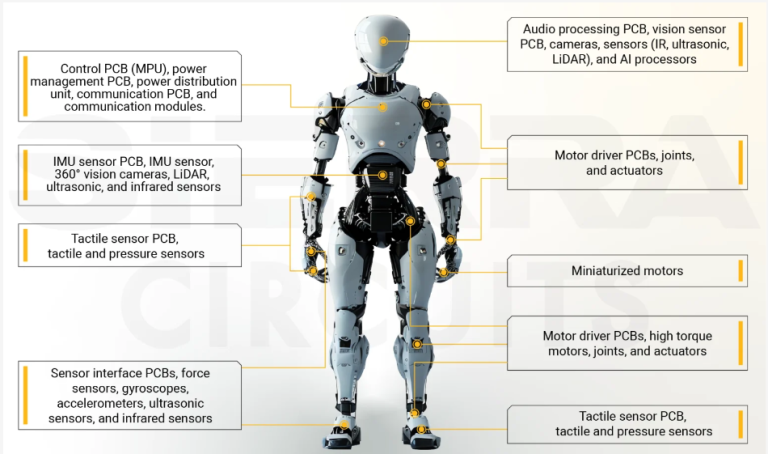
Interesting facts about PCBs
There is no doubt that the printed circuit board (PCB) is a milestone tool in human technology. Why? This is because it is hidden in every electronic device today. Like other great inventions in history, PCB has gradually matured with the advancement of the wheel of history. It has a history of 130 years and is the most beautiful scenery in the wheel of the industrial revolution.
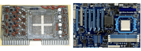
PCB has become a means to optimize the production process of electronic devices. Those electronic devices that used to be handmade have to be replaced by PCBs. This is because more functions will be integrated on the circuit board. The following pictures are the circuit board in the calculator in 1968 and the modern computer motherboard.
Here are ten interesting facts about PCBs.
Color
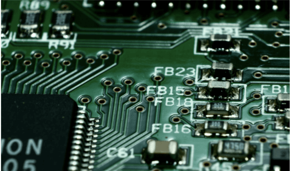
Even for some people who don’t know what PCBs are, they generally know what PCBs look like. They at least look like a traditional style, that is, its green color. This green is actually the color of the light-transmitting glass paint of the solder mask. Although the name of the solder mask is solder mask, its main function is to protect the covered circuits from moisture and dust.
As for why the solder mask is green, the main reason is that green is considered to be the military protection standard. Solder mask was first used in PCBs in military equipment to protect the reliability of circuits in the field, and green is the natural protective color in the military. Some people also believe that the color of the epoxy resin used in the original solder mask paint is green, so it has been used to this day.
Now the colors of solder mask are diverse, including black, red, yellow, etc. After all, green is not an industrial standard. As shown in the colorful PCB in the figure below.

Who invented PCB first
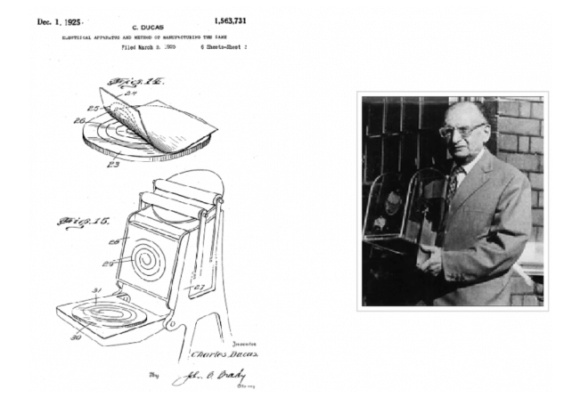
If you ask who invented printing, this honor belongs to Bi Sheng in the Northern Song Dynasty of China. But the earliest printed circuit board needs to be traced back to the Austrian engineer Charles Ducas who proposed the concept of using ink to conduct electricity (printing brass wires on the bottom board) in 1920. He used electroplating technology to directly generate wires on the surface of the insulator to produce a prototype of the PCB.
The metal wires on the original circuit board were brass, an alloy of copper and zinc. This subversive invention eliminated the complex wiring process of electronic circuits and ensured the reliability of circuit performance. This process did not enter the practical application stage until the end of World War II. The picture below is Charles Ducas and his printed circuit board patent.
Marking
There are also a lot of white markings on green circuit boards. For many years, people didn’t understand why these white printed markings were called “silk screen layers”. They are mainly used to identify the information of components on the circuit board and other circuit board related content.
This information was originally printed on the circuit board by screen printing, so it was called silk screen layer. Now it is done with special inkjet printers. This information can help circuit engineers check whether there are faults in the circuit board.

Components
The function of the circuit board is mainly completed by effectively connecting the components according to the schematic diagram. Each component has its own unique function. Even two devices that are close to each other on the circuit board may be very different. The types of devices basically include resistors, diodes, transistors, capacitors, relays, batteries, transformers and other miscellaneous (such as fuses, inductors, potentiometers, etc.).
Everywhere
It is no exaggeration to say that PCBs are everywhere. From computers to digital clocks, microwave ovens to televisions and stereo systems. If it is an electronic item or device, there is a 99% chance that it contains a PCB. So we may take it for granted that no electronic device can function without a PCB.
NASA
NASA has used groundbreaking technology in many of its projects. In the 1960s, NASA used PCBs on the Apollo 11 rocket because PCB-based electronic devices were lightweight and consumed little power. That was mankind’s greatest moment, sending astronauts to the moon for the first time. PCBs were responsible for this.
Surface Mount Technology (SMT)
Surface mount technology has brought PCBs into the modern era. Compared to the previous socket mounting method, this surface mount technology first uses special glue to stick the device on the PCB, and then uses special reflow soldering to electrically connect the device to the circuit board.
Rapid Prototyping PCB
During local experiments on circuits, breadboards, perforated boards, and other general-purpose circuit boards can be used for testing. With the increase of surface mounted components, new rapid PCB prototyping technologies have also emerged, such as thermal transfer PCB, 3D printed multi-layer circuit boards, etc. The picture below is a 3D printed circuit board.
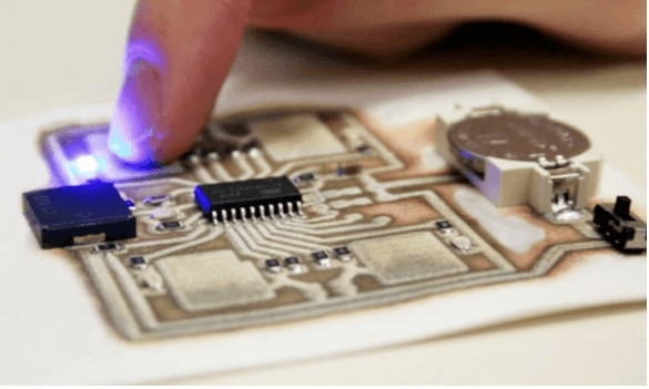
Soft PCB
PCBs are not all flat and hard. There are many soft PCBs working in many compact electronic devices. They often constitute application circuits in many movable joints, or form multi-layer three-dimensional circuits. The picture below is a transparent and soft PCB.

World’s largest PCB
The world’s largest PCB comes from the flexible multi-layer circuit board used in unmanned solar aircraft from Johnson Electronics in the UK. It is about 28 meters long. The circuit board made of soft polyimide as the base has better heat dissipation and higher conductive density. Such a long circuit board is made by etching in sections through a special production process. The longest flexible circuit board is shown in the figure below.