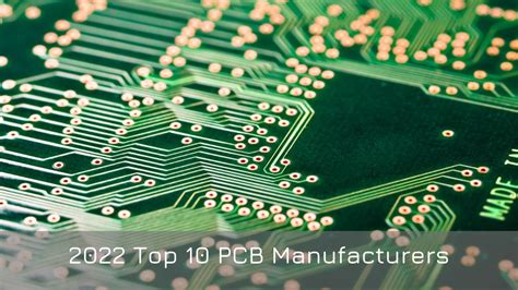
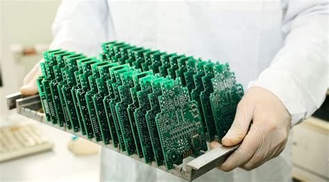
Introduction to PCBA: The Heart of Modern Electronics
Printed Circuit Board Assembly (PCBA) is a critical process in the manufacturing of electronic devices. It involves the assembly of various electronic components onto a printed circuit board (PCB) to create a functional electronic circuit. PCBA is the backbone of modern electronics, enabling the creation of everything from simple consumer gadgets to complex industrial machinery. This article delves into the intricacies of PCBA, exploring its processes, technologies, challenges, and future trends.
1. Understanding PCBA
1.1 What is PCBA?
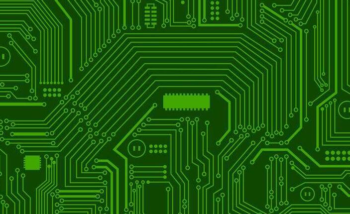
PCBA, or Printed Circuit Board Assembly, is the process of attaching electronic components to a PCB. The PCB itself is a flat board made of insulating material, such as fiberglass, with conductive pathways etched or printed onto its surface. These pathways, known as traces, connect the various components to form an electronic circuit.
1.2 Components of a PCBA
A typical PCBA consists of several key components:
- Resistors: These components limit the flow of electric current.
- Capacitors: They store and release electrical energy.
- Inductors: These components store energy in a magnetic field.
- Diodes: They allow current to flow in one direction only.
- Transistors: These are used to amplify or switch electronic signals.
- Integrated Circuits (ICs): These are complex circuits miniaturized into a single chip.
- Connectors: They provide interfaces for connecting the PCB to other devices or components.
2. The PCBA Process
The PCBA process involves several stages, each requiring precision and expertise. The main steps include:
2.1 Design and Layout
The first step in PCBA is designing the circuit and creating the PCB layout. This involves using specialized software to create a schematic diagram of the circuit, which is then converted into a physical layout of the PCB. The layout must consider factors such as component placement, trace routing, and thermal management.
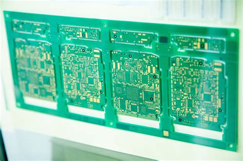
2.2 PCB Fabrication
Once the design is finalized, the PCB is fabricated. This involves several sub-steps:
- Substrate Preparation: The base material, usually fiberglass, is prepared.
- Copper Cladding: A thin layer of copper is laminated onto the substrate.
- Etching: The copper is etched away to create the desired circuit pattern.
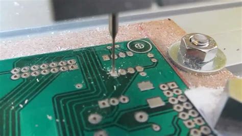
- Drilling: Holes are drilled for through-hole components and vias.
- Plating: The holes are plated with copper to ensure electrical connectivity.
- Solder Mask Application: A protective layer is applied to prevent solder bridges and short circuits.
- Silkscreen Printing: Labels and identifiers are printed on the PCB for easy assembly and troubleshooting.
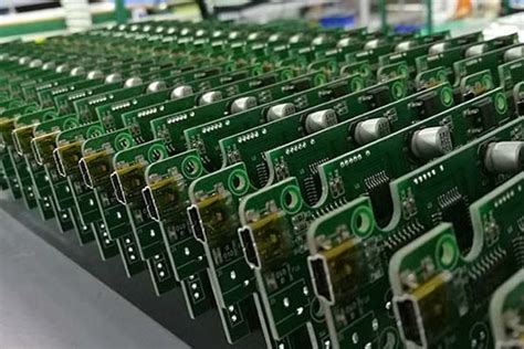
2.3 Component Placement
After the PCB is fabricated, the next step is placing the electronic components onto the board. This can be done manually or using automated machines, depending on the complexity and volume of production.
- Surface Mount Technology (SMT): Components are placed directly onto the surface of the PCB. This method is widely used due to its efficiency and ability to accommodate smaller components.
- Through-Hole Technology (THT): Components with leads are inserted into pre-drilled holes on the PCB. This method is used for larger components or those requiring stronger mechanical bonds.
2.4 Soldering
Soldering is the process of attaching the components to the PCB using solder, a metal alloy that melts at a relatively low temperature. There are two main soldering methods:
- Reflow Soldering: Used for SMT components, where solder paste is applied to the PCB, and the entire board is heated in a reflow oven to melt the solder.
- Wave Soldering: Used for THT components, where the PCB is passed over a wave of molten solder, which attaches the components to the board.
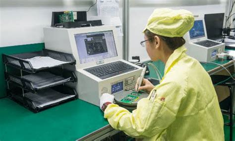
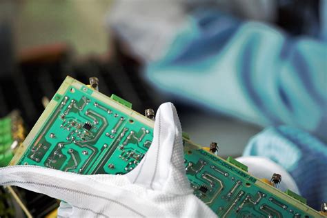
2.5 Inspection and Testing
After soldering, the PCBA undergoes rigorous inspection and testing to ensure quality and functionality.
- Visual Inspection: Technicians or automated systems check for visible defects such as solder bridges, misaligned components, or missing parts.
- Automated Optical Inspection (AOI): Cameras and software are used to detect defects that may not be visible to the naked eye.
- X-Ray Inspection: Used to inspect hidden solder joints, such as those under Ball Grid Array (BGA) components.
- Functional Testing: The assembled PCB is tested to ensure it performs as intended. This may involve powering up the board and running diagnostic software.
2.6 Cleaning and Coating
After inspection and testing, the PCBA is cleaned to remove any flux residues or contaminants. In some cases, a protective coating is applied to protect the board from environmental factors such as moisture, dust, and corrosion.
3. Challenges in PCBA
Despite advancements in technology, PCBA is not without its challenges. Some of the common issues include:
3.1 Miniaturization
As electronic devices become smaller and more compact, the components used in PCBA must also shrink in size. This poses challenges in terms of component placement, soldering, and inspection.
3.2 Thermal Management
High-density PCBs with numerous components generate significant heat, which can affect performance and reliability. Effective thermal management is crucial to prevent overheating and ensure the longevity of the device.
3.3 Component Availability
The global supply chain for electronic components can be unpredictable, leading to shortages or delays in obtaining necessary parts. This can disrupt production schedules and increase costs.
3.4 Quality Control
Ensuring the quality of each PCBA is critical, as even minor defects can lead to device failure. Implementing robust quality control measures is essential to maintain high standards.
4. Future Trends in PCBA
The field of PCBA is constantly evolving, driven by advancements in technology and changing market demands. Some of the key trends shaping the future of PCBA include:
4.1 Automation and Industry 4.0
The integration of automation and smart manufacturing techniques, often referred to as Industry 4.0, is transforming PCBA. Automated assembly lines, robotic soldering, and AI-driven inspection systems are becoming more prevalent, increasing efficiency and reducing human error.
4.2 Advanced Materials
The development of new materials, such as flexible and stretchable substrates, is enabling the creation of innovative PCBA designs. These materials allow for the production of flexible electronics, which can be used in wearable devices, medical implants, and other applications.
4.3 3D Printing
3D printing technology is being explored for PCB fabrication, allowing for rapid prototyping and customization. This could revolutionize the way PCBs are designed and manufactured, reducing lead times and costs.
4.4 Internet of Things (IoT)
The proliferation of IoT devices is driving demand for more complex and interconnected PCBA. IoT devices often require compact, low-power, and high-performance PCBs, pushing the boundaries of traditional PCBA techniques.
4.5 Environmental Sustainability
As environmental concerns grow, there is increasing pressure to make PCBA more sustainable. This includes using eco-friendly materials, reducing waste, and implementing recycling programs for electronic components.
5. Conclusion
PCBA is a vital process in the production of modern electronic devices, enabling the creation of complex circuits that power our daily lives. From design and fabrication to assembly and testing, each step in the PCBA process requires precision and expertise. Despite the challenges, advancements in technology and emerging trends are shaping the future of PCBA, making it more efficient, innovative, and sustainable. As the demand for electronic devices continues to grow, the importance of PCBA in the electronics industry will only increase, solidifying its role as the heart of modern electronics.