Is there any difference in PCB surface process?
1. Introduction
As human beings’ requirements for living environment continue to increase, the environmental issues involved in the current PCB production process are particularly prominent. At present, the topic of lead and bromine is the hottest; lead-free and halogen-free will affect the development of PCB in many ways. Although at present, the changes in the surface treatment process of PCB are not very large, it seems to be a relatively distant thing, but it should be noted that long-term slow changes will lead to huge changes. With the increasing calls for environmental protection, the surface treatment process of PCB will definitely change dramatically in the future.
2. Purpose of surface treatment
The most basic purpose of surface treatment is to ensure good solderability or electrical properties. Since copper in nature tends to exist in the form of oxides in the air and is unlikely to remain as original copper for a long time, other treatments are required for copper. Although strong flux can be used to remove most copper oxides in subsequent assembly, strong flux itself is not easy to remove, so the industry generally does not use strong flux.
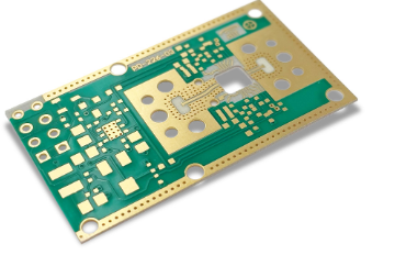
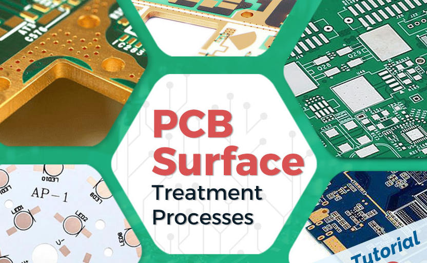
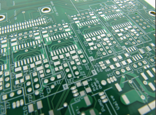
3. Five common surface treatment processes
There are many PCB surface treatment processes now, the most common ones are hot air leveling, organic coating, chemical nickel plating/immersion gold, immersion silver and immersion tin. The following will introduce them one by one.
(1).Hot air leveling
Hot air leveling, also known as hot air solder leveling, is a process of coating molten tin-lead solder on the surface of the PCB and leveling (blowing) it with heated compressed air to form a coating layer that is both resistant to copper oxidation and provides good solderability. During hot air leveling, solder and copper form copper-tin intermetallic compounds at the junction. The thickness of the solder protecting the copper surface is about 1-2 mil.
The PCB is immersed in molten solder during hot air leveling; the wind knife blows the liquid solder flat before the solder solidifies; the wind knife can minimize the meniscus of the solder on the copper surface and prevent solder bridging. Hot air leveling is divided into vertical and horizontal types. It is generally believed that the horizontal type is better, mainly because the horizontal hot air leveling coating is more uniform and can realize automated production. The general process of hot air leveling is: micro-etching → preheating → flux coating → tin spraying → cleaning.
(2).Organic coating
The organic coating process is different from other surface treatment processes. It acts as a barrier layer between copper and air; the organic coating process is simple and low-cost, which makes it widely used in the industry. The early organic coating molecules were imidazole and benzophenone, which played a rust-proof role. The latest molecules are mainly benzimidazole, which is chemically bonded to the copper on the PCB. In the subsequent welding process, if there is only one layer of organic coating on the copper surface, it will not work. There must be many layers. This is why copper liquid is usually added to the chemical tank. After the first layer is coated, the coating layer absorbs copper; then the second layer of organic coating molecules combines with copper, until twenty or even hundreds of organic coating molecules gather on the copper surface, which can ensure multiple reflow soldering. Experiments show that the latest organic coating process can maintain good performance during multiple lead-free soldering processes.
The general process of organic coating is: degreasing → micro-etching → pickling → pure water cleaning → organic coating → cleaning. The process control is relatively easy compared to other surface treatment processes.
(3).Chemical nickel plating / immersion gold
The chemical nickel plating / immersion gold process is not as simple as organic coating. Chemical nickel plating / immersion gold seems to put on thick armor for PCB. In addition, the chemical nickel plating / immersion gold process is not like organic coating as an anti-rust barrier. It can be useful and achieve good electrical properties during the long-term use of PCB. Therefore, chemical nickel plating / immersion gold is to wrap a thick layer of nickel-gold alloy with good electrical properties on the copper surface, which can protect PCB for a long time. In addition, it also has environmental tolerance that other surface treatment processes do not have. The reason for nickel plating is that gold and copper will diffuse with each other, and the nickel layer can prevent the diffusion between gold and copper; if there is no nickel layer, gold will diffuse into copper within hours. Another advantage of chemical nickel plating / immersion gold is the strength of nickel. Nickel with a thickness of only 5 microns can limit the expansion in the Z direction at high temperature. In addition, chemical nickel plating/immersion gold can also prevent the dissolution of copper, which will be beneficial to lead-free assembly.
The general process of chemical nickel plating/immersion gold plating is: acid cleaning → micro-etching → pre-immersion → activation → chemical nickel plating → chemical immersion gold. There are mainly 6 chemical tanks, involving nearly 100 chemicals, so process control is more difficult.
(4).Immersion silver
The immersion silver process is between organic coating and chemical nickel plating/immersion gold plating. The process is relatively simple and fast; it is not as complicated as chemical nickel plating/immersion gold plating, nor does it put a thick layer of armor on the PCB, but it can still provide good electrical properties. Silver is the little brother of gold. Even if exposed to heat, humidity and pollution, silver can still maintain good solderability, but it will lose its luster. Immersion silver does not have the good physical strength of chemical nickel plating/immersion gold because there is no nickel under the silver layer. In addition, immersion silver has good storage properties, and there will be no major problems in assembly after immersion silver for a few years.
Immersion silver is a replacement reaction, which is almost a submicron pure silver coating. Sometimes some organic matter is included in the silver immersion process, mainly to prevent silver corrosion and eliminate silver migration problems; it is generally difficult to measure this thin layer of organic matter, and analysis shows that the weight of the organic matter is less than 1%.
(5).Tin immersion
Since all current solders are based on tin, the tin layer can match any type of solder. From this point of view, the tin immersion process has great development prospects. However, tin whiskers appeared in the previous PCB after the tin immersion process. Tin whiskers and tin migration will bring reliability problems during the welding process, so the adoption of the tin immersion process is limited. Later, organic additives were added to the tin immersion solution, which can make the tin layer structure granular, overcoming the previous problems, and also has good thermal stability and solderability.
The tin immersion process can form a flat copper-tin intermetallic compound. This feature makes the tin immersion have the same good solderability as hot air leveling without the headache of hot air leveling. Tin immersion also does not have the diffusion problem between chemical nickel plating/immersion gold metals-copper-tin intermetallic compounds can be firmly combined. Tin immersion boards cannot be stored for too long, and assembly must be carried out according to the order of tin immersion.
(6).Other surface treatment processes
Other surface treatment processes are less used. Let’s take a look at the relatively more widely used electroplating nickel-gold and chemical palladium plating processes.
Electroplating nickel-gold is the originator of PCB surface treatment processes. It has been around since the emergence of PCBs and has gradually evolved into other methods. It is to first plate a layer of nickel on the conductor on the surface of the PCB and then plate a layer of gold. Nickel plating is mainly to prevent the diffusion between gold and copper. There are two types of electroplating nickel-gold now: soft gold plating (pure gold, the gold surface does not look bright) and hard gold plating (the surface is smooth and hard, wear-resistant, contains other elements such as cobalt, and the gold surface looks brighter). Soft gold is mainly used for gold wire during chip packaging; hard gold is mainly used for electrical interconnection at non-welding locations.
Considering the cost, the industry often uses image transfer to perform selective electroplating to reduce the use of gold. At present, the use of selective electroplating gold in the industry continues to increase, mainly because the process control of chemical nickel plating/immersion gold is relatively difficult.
Under normal circumstances, welding will cause electroplated gold to become brittle, which will shorten the service life, so welding on electroplated gold should be avoided; but chemical nickel plating/immersion gold rarely becomes brittle because the gold is very thin and consistent.
The process of chemical palladium plating is similar to that of chemical nickel plating. The main process is to reduce palladium ions to palladium on the catalytic surface through a reducing agent (such as sodium dihydrogen hypophosphite). The newly formed palladium can become a catalyst to promote the reaction, so a palladium coating of any thickness can be obtained. The advantages of chemical palladium plating are good welding reliability, thermal stability, and surface flatness.
4.Selection of surface treatment process
The selection of surface treatment process mainly depends on the type of final assembly components; the surface treatment process will affect the production, assembly and final use of PCBs. The following will specifically introduce the use occasions of the five common surface treatment processes.
(1)Hot air leveling
Hot air leveling once dominated the PCB surface treatment process. In the 1980s, more than three-quarters of PCBs used hot air leveling, but the industry has been reducing the use of hot air leveling over the past decade. It is estimated that about 25%-40% of PCBs currently use hot air leveling. Hot air leveling is dirty, smelly, and dangerous, so it has never been a popular process, but it is an excellent process for larger components and larger wires. In high-density PCBs, the flatness of hot air leveling will affect subsequent assembly; therefore, HDI boards generally do not use hot air leveling. With the advancement of technology, the industry has now developed hot air leveling processes suitable for assembling QFP and BGA with smaller spacing, but there are few actual applications. At present, some factories use organic coating and chemical nickel/immersion gold plating processes to replace hot air leveling processes; technological developments have also led some factories to use immersion tin and immersion silver processes. Coupled with the trend of lead-free in recent years, the use of hot air leveling is further restricted. Although the so-called lead-free hot air leveling has appeared, this may involve equipment compatibility issues.
(2)Organic coating
It is estimated that about 25%-30% of PCBs currently use organic coating technology, and this proportion has been rising (it is very likely that organic coating has now surpassed hot air leveling and ranked first). Organic coating technology can be used on low-tech PCBs as well as high-tech PCBs, such as PCBs for single-sided TVs and boards for high-density chip packaging. For BGA, organic coating is also widely used. If the PCB does not have surface connection functional requirements or storage period restrictions, organic coating will be the most ideal surface treatment process.
(3)Chemical nickel plating/immersion gold
Different from organic coating, chemical nickel plating/immersion gold process is mainly used on boards with surface connection functional requirements and longer storage period, such as mobile phone keypad area, router shell edge connection area and chip processor elastic connection electrical contact area. Due to the flatness problem of hot air leveling and the problem of removing organic coating flux, chemical nickel plating/immersion gold was widely used in the 1990s; later, due to the emergence of black disks and brittle nickel-phosphorus alloys, the application of chemical nickel plating/immersion gold process has decreased, but now almost every high-tech PCB factory has chemical nickel plating/immersion gold line. Considering that the solder joints will become brittle when the copper-tin intermetallic compound is removed, many problems will occur at the relatively brittle nickel-tin intermetallic compound. Therefore, portable electronic products (such as mobile phones) almost all use copper-tin intermetallic compound solder joints formed by organic coating, immersion silver or immersion tin, and chemical nickel plating/immersion gold is used to form the key area, contact area and EMI shielding area. It is estimated that about 10%-20% of PCBs currently use chemical nickel plating/immersion gold process.
(4)Immersion silver
Immersion silver is cheaper than chemical nickel plating/immersion gold. If the PCB has connection functional requirements and needs to reduce costs, immersion silver is a good choice; coupled with the good flatness and contact of immersion silver, the immersion silver process should be selected. Immersion silver is widely used in communication products, automobiles, and computer peripherals, and is also used in high-speed signal design. Since immersion silver has good electrical properties that other surface treatments cannot match, it can also be used in high-frequency signals. EMS recommends the use of immersion silver because it is easy to assemble and has good inspectability. However, due to defects such as loss of gloss and solder joint voids, immersion silver has slowed down its growth (but not decreased). It is estimated that about 10%-15% of PCBs currently use immersion silver.
(5)Immersion tin
Tin has been introduced into the surface treatment process for nearly ten years. The emergence of this process is the result of the requirements of production automation. Immersion tin does not bring any * elements into the welding point, and is particularly suitable for communication backplanes. Tin will lose solderability outside the storage period of the board, so immersion tin requires better storage conditions. In addition, the immersion tin process is restricted because it contains carcinogens. It is estimated that about 5%-10% of PCBs currently use the immersion tin process.