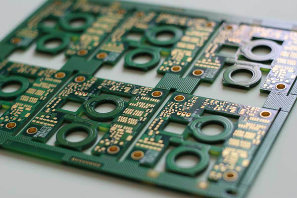
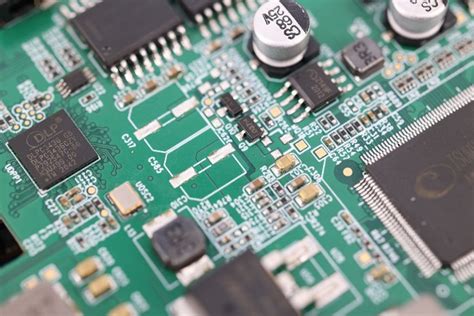
It is a printed circuit board
History And Evolution Of Printed Circuit Boards
The history and evolution of printed circuit boards (PCBs) is a fascinating journey that reflects the broader advancements in technology and electronics over the past century. Initially, electronic circuits were constructed using point-to-point wiring, a labor-intensive process that involved manually connecting each component with wires. This method, while effective for early electronic devices, was not sustainable as the demand for more complex and reliable electronics grew. The need for a more efficient solution led to the development of the printed circuit board, a pivotal innovation that revolutionized the electronics industry.
The concept of a printed circuit board can be traced back to the early 20th century.
In 1903, German inventor Albert Hanson filed a patent for a flat foil conductor laminated to an insulating board, a rudimentary precursor to the modern PCB. However, it was not until the 1940s that PCBs began to gain significant traction. During World War II, the United States military sought a more reliable and compact way to produce radio sets, which led to the adoption of PCBs. The use of PCBs allowed for mass production and improved reliability, as the circuits were less prone to human error and mechanical failure compared to their wired counterparts.
Following the war, the commercial electronics industry quickly recognized the advantages of PCBs.
The 1950s and 1960s saw a rapid expansion in their use, driven by the burgeoning consumer electronics market. During this period, significant advancements were made in PCB manufacturing techniques. The introduction of the photoengraving process allowed for more precise and intricate circuit designs, while the development of multilayer PCBs enabled the creation of more compact and complex electronic devices. These innovations were crucial in supporting the miniaturization trend that characterized the electronics industry during the latter half of the 20th century.
As technology continued to advance, so too did the complexity and capabilities of PCBs.
The 1970s and 1980s witnessed the rise of surface mount technology (SMT), which allowed components to be mounted directly onto the surface of the board rather than being inserted through holes.
This development further reduced the size and weight of electronic devices, paving the way for the proliferation of personal computers, mobile phones, and other portable electronics. The integration of SMT with automated assembly processes also significantly increased production efficiency and reduced costs.
In recent decades, the evolution of PCBs has been driven by the demand for even greater functionality and performance.
The advent of high-density interconnect (HDI) technology has enabled the production of PCBs with extremely fine traces and spaces, allowing for the integration of more components in a smaller area.
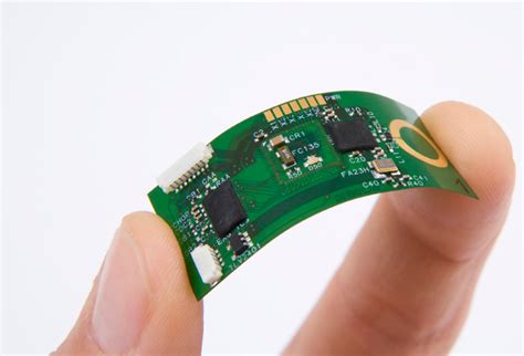
This has been particularly important in the development of modern smartphones and wearable devices, where space is at a premium. Additionally, advancements in materials science have led to the creation of flexible and rigid-flex PCBs, which offer greater design versatility and are increasingly used in applications where traditional rigid boards are unsuitable.
In conclusion, the history and evolution of printed circuit boards is a testament to the relentless pursuit of innovation in the electronics industry. From their humble beginnings as a solution to the limitations of point-to-point wiring, PCBs have become an indispensable component of modern technology. As we continue to push the boundaries of what is possible in electronics, it is certain that PCBs will remain at the forefront of this exciting journey, continually adapting to meet the ever-changing demands of the digital age.

The Manufacturing Process Of Printed Circuit Boards
The manufacturing process of printed circuit boards (PCBs) is a complex and intricate procedure that involves several stages, each crucial to the creation of a functional and reliable electronic component.
Initially, the process begins with the design phase, where engineers use specialized software to create a detailed schematic of the circuit.
This schematic serves as a blueprint, guiding the subsequent steps in the manufacturing process.
Once the design is finalized, it is converted into a format suitable for production, typically a Gerber file, which contains all the necessary information about the board’s layout, including the placement of components and the routing of electrical connections.
Following the design phase, the next step is the selection of materials.
The most common substrate used in PCB manufacturing is a fiberglass-reinforced epoxy laminate, known as FR-4. This material is chosen for its excellent insulating properties and mechanical strength. Copper is then laminated onto the substrate to form the conductive pathways. The thickness of the copper layer can vary depending on the specific requirements of the PCB, with thicker layers used for boards that need to handle higher currents.
Once the materials are prepared, the process of transferring the circuit design onto the substrate begins.
This is typically achieved through a method called photolithography. In this process, a photosensitive film, known as a photoresist, is applied to the copper-clad substrate. The Gerber file is then used to create a photomask, which is placed over the photoresist-coated board. When exposed to ultraviolet light, the photoresist hardens in areas not covered by the mask, creating a pattern that mirrors the circuit design. The unhardened photoresist is then washed away, leaving behind a precise pattern of the circuit on the copper layer.
Subsequently, the board undergoes an etching process, where a chemical solution is used to remove the exposed copper, leaving only the desired circuit pattern intact.
This step is critical, as it defines the electrical pathways that will connect the various components on the PCB. After etching, the remaining photoresist is stripped away, revealing the finished copper traces.
The next phase involves drilling holes into the board for component leads and vias, which are used to connect different layers of a multilayer PCB. Precision drilling machines equipped with tiny drill bits are employed to ensure accuracy and consistency. Once the holes are drilled, they are plated with copper to establish electrical connections between layers.
Following drilling and plating, the board is coated with a solder mask, a protective layer that insulates the copper traces and prevents solder bridges during component assembly.
The solder mask is typically green, although other colors are available. Silkscreen printing is then applied to add labels and markings, aiding in component placement and identification.
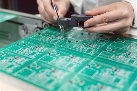
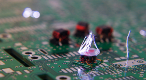
Finally, the PCB undergoes a series of inspections and tests to ensure its functionality and reliability. These tests may include electrical testing to verify connectivity and impedance, as well as visual inspections to check for defects. Once the board passes all quality control measures, it is ready for assembly, where electronic components are soldered onto the board to create a complete electronic device. Through this meticulous process, printed circuit boards are manufactured to meet the high standards required for modern electronic applications.

Applications And Uses Of Printed Circuit Boards In Modern Technology
Printed circuit boards (PCBs) are integral components in the realm of modern technology, serving as the backbone for a multitude of electronic devices. Their applications and uses are vast, spanning across various industries and sectors, each benefiting from the unique advantages that PCBs offer. To begin with, the consumer electronics industry heavily relies on PCBs to function efficiently. Devices such as smartphones, tablets, and laptops are all built upon the foundation of PCBs, which provide the necessary pathways for electrical currents to flow between components. This ensures that these devices operate smoothly, delivering the high performance that users have come to expect.
In addition to consumer electronics, the automotive industry has also embraced the use of PCBs.
Modern vehicles are equipped with numerous electronic systems, from engine management units to advanced driver-assistance systems (ADAS). These systems depend on PCBs to manage and control various functions, enhancing both the safety and efficiency of vehicles. As the automotive industry continues to evolve towards electric and autonomous vehicles, the demand for more sophisticated PCBs is expected to rise, further cementing their importance in this sector.
Moreover, the medical field has seen significant advancements due to the integration of PCBs in medical devices.
Equipment such as MRI machines, heart monitors, and even portable medical devices like insulin pumps rely on PCBs to function accurately and reliably. The precision and reliability offered by PCBs are crucial in medical applications, where even the slightest error can have serious consequences. As medical technology continues to advance, the role of PCBs in developing innovative solutions for patient care will undoubtedly expand.
Furthermore, the telecommunications industry is another area where PCBs play a critical role.
With the ever-growing demand for faster and more reliable communication networks, PCBs are essential in the development of infrastructure such as routers, switches, and satellite systems. These components are vital for maintaining the seamless connectivity that modern society depends on, enabling everything from simple phone calls to complex data transfers across the globe.
In the realm of industrial applications, PCBs are utilized in a wide array of machinery and equipment.
From manufacturing plants to power generation facilities, PCBs are used to control and monitor processes, ensuring that operations run smoothly and efficiently. The ability of PCBs to withstand harsh environments and operate under extreme conditions makes them ideal for industrial use, where durability and reliability are paramount.
Additionally, the aerospace and defense sectors benefit significantly from the use of PCBs.
In these industries, the need for robust and reliable electronic systems is critical, as they are often subjected to extreme conditions and high-stress environments. PCBs are used in everything from navigation systems to communication devices, playing a vital role in ensuring the safety and success of missions.
In conclusion, the applications and uses of printed circuit boards in modern technology are extensive and varied. From consumer electronics to aerospace, PCBs are indispensable components that enable the functionality and advancement of numerous technologies. As technology continues to evolve, the role of PCBs will undoubtedly expand, driving innovation and shaping the future of various industries. Their versatility, reliability, and efficiency make them a cornerstone of modern technological development, underscoring their significance in our increasingly digital world.
Environmental Impact And Recycling Of Printed Circuit Boards
Printed circuit boards (PCBs) are integral components of modern electronic devices, serving as the backbone for connecting various electronic components. However, the environmental impact of PCBs is a growing concern, given the rapid pace of technological advancement and the corresponding increase in electronic waste. Understanding the environmental implications of PCBs and exploring effective recycling methods are crucial steps toward mitigating their negative effects.
The production of PCBs involves several processes that can have significant environmental consequences.
The manufacturing process requires the use of various chemicals, including acids and solvents, which can lead to hazardous waste if not properly managed. Additionally, the etching process, which creates the intricate pathways on the board, often results in the release of toxic substances. These chemicals, if not disposed of correctly, can contaminate soil and water sources, posing risks to ecosystems and human health.
Moreover, PCBs are composed of multiple materials, including metals such as copper, lead, and tin, as well as non-metallic substances like fiberglass and epoxy resins.
The extraction and processing of these materials contribute to environmental degradation. For instance, mining for metals can lead to habitat destruction and pollution, while the production of fiberglass and resins involves energy-intensive processes that contribute to greenhouse gas emissions. Consequently, the environmental footprint of PCBs extends beyond their immediate production, encompassing the broader impacts of resource extraction and material processing.
As electronic devices become obsolete at an increasing rate, the disposal of PCBs presents another environmental challenge.
When discarded improperly, PCBs contribute to the growing problem of electronic waste, or e-waste, which is one of the fastest-growing waste streams globally. E-waste often ends up in landfills, where toxic substances can leach into the environment, or is incinerated, releasing harmful emissions into the atmosphere. These practices not only harm the environment but also result in the loss of valuable materials that could be recovered and reused.
Recycling PCBs is a critical component of addressing their environmental impact.
Effective recycling processes can recover valuable metals and reduce the need for virgin material extraction, thereby conserving natural resources and minimizing environmental harm. Mechanical separation, pyrometallurgical, and hydrometallurgical processes are among the methods used to recycle PCBs. Mechanical separation involves shredding and sorting the materials, while pyrometallurgical processes use high temperatures to extract metals. Hydrometallurgical methods, on the other hand, employ chemical solutions to dissolve and recover metals.
Despite the potential benefits, PCB recycling faces several challenges.
The complexity of PCBs, with their diverse material composition, makes recycling a technically demanding process. Additionally, the economic viability of recycling is often contingent on the fluctuating market prices of recovered materials. To overcome these challenges, advancements in recycling technology and supportive policy frameworks are essential. Governments and industries must collaborate to develop efficient recycling systems and promote sustainable practices.
In conclusion, while PCBs are indispensable to modern electronics, their environmental impact cannot be overlooked.
From production to disposal, PCBs pose significant environmental challenges that necessitate comprehensive solutions. By enhancing recycling efforts and adopting sustainable practices, it is possible to mitigate the adverse effects of PCBs and contribute to a more sustainable future. As society continues to rely on electronic devices, addressing the environmental impact of PCBs will remain a critical issue that demands ongoing attention and innovation.