Key Considerations in PCB Manufacturing: Three Critical Aspects to Ensure Quality and Efficiency
Printed Circuit Board (PCB) manufacturing is a complex process that requires meticulous attention to detail to ensure functionality, reliability, and cost-effectiveness. Whether producing simple single-layer boards or advanced multi-layer high-density interconnect (HDI) PCBs, manufacturers must carefully evaluate design, material selection, fabrication processes, and quality control. This article explores the three most crucial aspects to consider in PCB production: Design and Layout Optimization, Material Selection and Compatibility, and Manufacturing Process Control. By addressing these key areas, manufacturers can enhance performance, reduce defects, and improve overall production efficiency.
1. Design and Layout Optimization
The foundation of a high-quality PCB lies in its design. A well-optimized layout ensures signal integrity, thermal management, and manufacturability while minimizing potential errors. Key considerations in PCB design include:
A. Signal Integrity and Electromagnetic Compatibility (EMC)
- Trace Routing: Proper trace width, spacing, and impedance control are essential to prevent signal degradation, crosstalk, and electromagnetic interference (EMI). High-speed designs require controlled impedance routing and differential pairs.
- Grounding and Power Planes: A solid ground plane reduces noise and improves EMC. Decoupling capacitors should be placed near power pins to stabilize voltage fluctuations.
- Via Placement: Excessive vias can increase inductance and signal loss. Blind and buried vias in HDI designs help optimize space but add complexity.
B. Thermal Management
- Copper Weight and Heat Dissipation: Thicker copper layers (e.g., 2 oz or more) improve current-carrying capacity and heat dissipation. Thermal vias and heatsinks help manage heat in high-power applications.
- Component Placement: Heat-generating components (e.g., processors, power regulators) should be spaced appropriately and placed near cooling mechanisms.
C. Design for Manufacturability (DFM)
- Minimum Trace/Space Requirements: Adhering to the manufacturer’s capabilities prevents fabrication issues.
- Solder Mask and Silkscreen Clarity: Clear markings prevent assembly errors, and proper solder mask application avoids bridging.
- Panelization: Efficient panel design maximizes material usage and facilitates automated assembly.
Failure to optimize design can lead to signal loss, overheating, or assembly defects, increasing costs and delays.
2. Material Selection and Compatibility
Choosing the right materials is critical for PCB performance, especially in demanding environments. Key factors include:
A. Substrate Materials
- FR-4: The most common material, suitable for standard applications. Variants with high Tg (glass transition temperature) offer better thermal resistance.
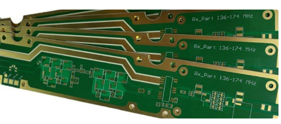
- High-Frequency Laminates (e.g., Rogers, PTFE): Essential for RF/microwave PCBs due to low dielectric loss.
- Flex and Rigid-Flex Materials (Polyimide): Used in flexible circuits, requiring careful handling to avoid cracking.
B. Copper Foil Quality
- Electrodeposited (ED) vs. Rolled Annealed (RA) Copper: ED copper is cost-effective for standard boards, while RA copper offers better flexibility for high-frequency applications.
- Surface Treatments: ENIG (Electroless Nickel Immersion Gold), HASL (Hot Air Solder Leveling), and OSP (Organic Solderability Preservative) affect solderability and shelf life.
C. Environmental and Reliability Factors
- Moisture Absorption: Materials like FR-4 can absorb moisture, leading to delamination during reflow. Pre-baking may be necessary.
- Thermal Expansion Coefficients (CTE): Mismatched CTE between layers can cause warping or via cracking in multilayer boards.
Incorrect material selection can result in premature failure, especially in harsh conditions (high temperature, humidity, or vibration).
3. Manufacturing Process Control
Precision in fabrication and assembly ensures consistency and reliability. Critical steps include:
A. Fabrication Process
- Photolithography and Etching: Accurate exposure and etching prevent trace defects (undercut or over-etch).
- Layer Alignment (Registration): Misalignment in multilayer PCBs can cause short circuits or open connections.
- Drilling and Plating: Laser drilling for microvias requires precision to avoid incomplete plating or hole wall damage.
B. Surface Finish Application
- HASL vs. ENIG vs. Immersion Silver: Each has trade-offs in cost, solderability, and durability. ENIG is preferred for fine-pitch components.
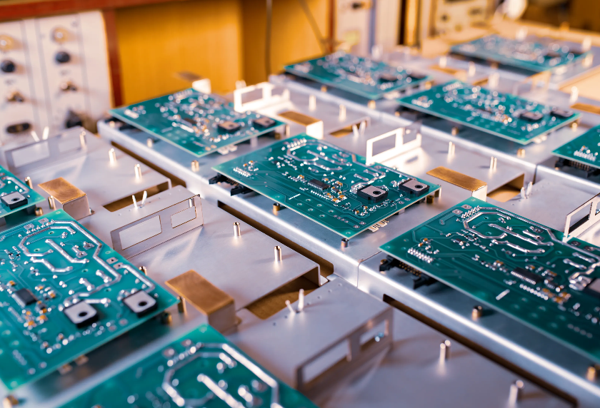
C. Quality Assurance and Testing
- Automated Optical Inspection (AOI): Detects soldering defects, missing components, or misalignment.
- Electrical Testing (Flying Probe or Bed of Nails): Verifies connectivity and detects shorts/open circuits.
- Environmental Stress Testing: Thermal cycling, vibration, and humidity tests validate reliability.
Process deviations can lead to costly rework or field failures, emphasizing the need for strict quality control.
Conclusion
Successful PCB manufacturing hinges on balancing design optimization, material selection, and process control. By prioritizing these three aspects, manufacturers can produce high-quality, reliable PCBs that meet performance requirements while minimizing defects and costs. Continuous advancements in materials and fabrication technologies further enhance PCB capabilities, enabling innovation in electronics across industries.
Investing in robust design tools, collaborating with experienced suppliers, and implementing rigorous quality checks will ensure that PCB production meets the highest standards in an increasingly competitive market.