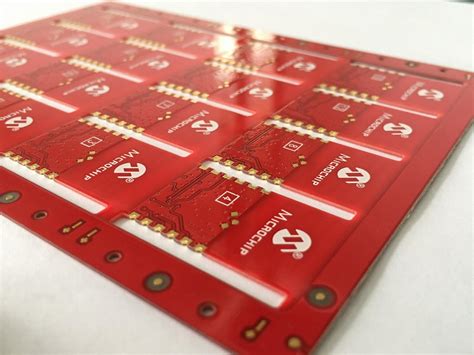
Key points for wet film application on circuit boards
1.Brushing boards
The materials provided by the previous process (i.e. production boards) are required to have no serious oxidation, oil stains, or wrinkles on the board surface. We use pickling (5% sulfuric acid) spraying to remove organic impurities and inorganic dirt, and then use a 500-mesh nylon brush roller to brush. After brushing the board, the following should be achieved: no oxidation on the copper surface, uniform roughening of the copper surface, strict flatness on the copper surface, and no water marks on the copper surface. This effect enhances the bonding force between the wet film and the copper foil surface to meet the requirements of subsequent process technology. The surface state of the copper foil after brushing the board directly affects the yield rate of the PCB.
2.Screen printing
In order to achieve the required thickness of the wet film, the screen should be selected before screen printing, and attention should be paid to the thickness and mesh count of the screen (i.e. the number of lines per unit length). The film thickness is related to the ink penetration of the screen. The theoretical ink penetration (Uth) of the ink is:
Uth=Dw2 (w+d)2 ×1000
(D ─ screen sand thickness d ─ wire diameter w ─ opening width)
The actual ink penetration is also related to the wet film viscosity, scraper pressure, and scraper moving speed. In order to achieve uniform coverage, the scraper blade should be well ground. The thickness of the post-printing plate film should be controlled between 15-25μm. If the film is too thick, it is easy to cause underexposure, poor development, difficult to control pre-drying, easy to cause battlefield film, and difficult to operate. If the film is too thin, it is easy to cause overexposure, good corrosion resistance, poor insulation during electroplating, and difficult to remove the film. To make fine lines below 0.15μm, the film should be less than 20μm after filming.
The viscosity of the wet film should be adjusted before use, and it should be fully stirred and left to stand for fifteen minutes. The environment of the screen printing room should be kept clean to prevent foreign debris from falling on the surface and affecting the qualified rate of the board. The temperature should be controlled at around 20℃ and the relative humidity should be around 50%.
3.Pre-baking
The pre-baking parameters are to bake the first side at 80-100℃ for 7-10 minutes, and the second side at 80-100℃ for 10-20 minutes. Pre-baking is mainly to evaporate the solvent in the ink, and pre-baking is related to the success or failure of wet film application. Insufficient pre-baking will make the board stick during storage and transportation, and stick to the film during exposure, eventually causing disconnection or short circuit; excessive pre-baking will make the development unclean and the line edge jagged. Pre-baking directly affects the quality of PCB, so it is important to test the thickness of the wet film frequently in normal operation, adjust the parameters of the oven according to the changes in ambient temperature, and frequently check whether the blowing and circulation systems of the oven are in good condition. The dried board should be exposed as soon as possible, preferably not more than 12 hours.
4.Exposure
Exposure is the photopolymerization reaction process produced by the monomer molecules in the wet film after absorbing light energy under the action of ultraviolet rays. Use a high-power exposure machine to reduce the exposure time and heat accumulation, ensure the stability of the exposed pattern and reduce sticking to the film. Keep the exposure room clean in each shift to prevent debris from adhering to the plate surface and causing sand eyes, gaps, and broken lines. Use an exposure ruler to adjust the exposure time to avoid excessive or insufficient exposure. The final exposure level should be controlled between 6-8 levels. When exposing, the same type of printed single board should be exposed at the same position as much as possible, and the energy of the same type of board should be the same as much as possible. If the exposure is too large, the anti-etching and anti-plating effects are better, but there are unsatisfactory film removal effects and the graphic circuit is reduced (using positive film) or enlarged (using negative film). Insufficient exposure causes poor development, poor corrosion resistance, hairy line edges, increased or decreased line spacing, and easy to cause short circuits or broken lines during etching.
5.Development
Development is the process of removing the unexposed wet film layer to obtain the required circuit pattern. Strictly control the concentration (10-12g/l) and temperature (30-34℃) of the developer. Too high or too low a concentration of the developer can easily cause incomplete development. Optimize the development speed to match it with the exposure amount, and clean the nozzle frequently to keep the nozzle pressure and distribution consistent. Too long a development time or too high a development temperature will cause degradation of the wet film surface, and severe penetration or side etching will occur during electroplating or acid etching, reducing the precision requirements for pattern production.
6.Etching and film removal
Etching finally obtains the circuit pattern we need. The etching solution can be alkaline ferric chloride, acidic cupric chloride and ammonia water. Different etching speeds should be used for different copper foil thicknesses during etching. The etching speed must also match the temperature and concentration of the etching solution. The nozzle of the etching machine should be maintained frequently to keep the pressure and spray distribution uniform, otherwise uneven etching and copper wires on the edge will be caused, affecting the quality of the PCB. Our company uses 4-7% sodium hydroxide solution at 50-60℃ to remove the film. The main process is that sodium hydroxide makes the film layer expand and then subdivide. If the parameters are well controlled, the wet film in the hole can also be removed. We use wet film to transfer patterns on special double-sided boards and achieve good results.


