Key Process Improvements for High-precision Printed Wiring Boards
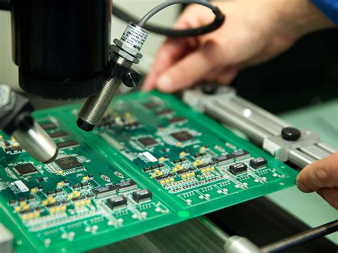
With the development of the electronics industry, the degree of integration of electronic components is getting higher and lower, and the volume is getting smaller and smaller, and BGA type packages are generally used.
Therefore, the PCB’s wiring will be smaller and smaller, with more and more layers. Reducing line width and line spacing is to use a limited area as much as possible, and increasing the number of layers is space utilization. The future line of the circuit board will be 2-3mil, or less.
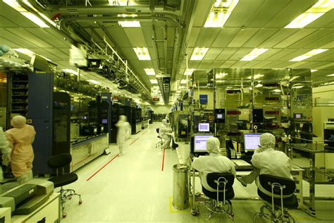
It is generally believed that every time a production circuit board is increased or raised by one grade, it must be invested once and the investment funds are relatively large.
In other words, high-end circuit boards are produced from high-end equipment. However, large-scale investment is not affordable for every company, and investing later to do experiments to collect process data, trial production takes a lot of time and money. It seems to be a better way to do tests and trial production according to the current situation of the company, and then decide whether to invest according to the actual situation and market conditions. This article details the limits of the width of fine lines that can be produced under normal equipment conditions, and the conditions and methods for the production of fine lines.
The general production process can be divided into cover hole acid etching and pattern plating, both have their own advantages and disadvantages.
The circuit obtained by the acid etching method is very uniform, which is conducive to impedance control, and the environmental pollution is small. However, if one hole is broken, it is scrapped. T
he production control of alkali corrosion is relatively easy, but the line is uneven and the environmental pollution is also large.
First of all, the main line of production is dry film, different dry film resolution is different but generally can display 2mil/2mil linewidth after exposure,1
ordinary exposure machine resolution can reach 2mil, generally in this There is no problem with the line width in the range. In the 4mil/4mil linewidth or above, the relationship between the pressure and the concentration of the syrup is not very large. Below the linewidth of 3mil/3mil, the nozzle is the key to the resolution. Generally, fan nozzles are used in the pressure. Around 3BAR can develop.
Although the exposure energy has a great influence on the circuit, most of the dry film used in the market today has a wide range of exposure.
In the 12-18 (25 exposure scale) or 7-9 (21 exposure scale) can be distinguished, in general, a little lower exposure energy is conducive to the resolution but the energy is too low when the air dust and miscellaneous The material has a great influence on it, and it will cause an open circuit (etching) or a short circuit (alkaline corrosion) in the subsequent process, so the actual production must be combined with the cleanliness of the darkroom so that the circuit board circuit that can be produced can be selected according to the actual situation. Minimum line width and line spacing.
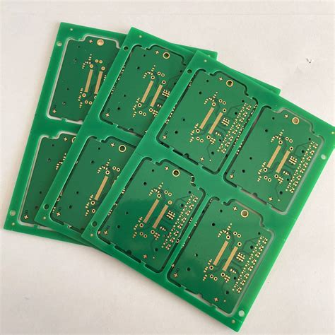
The effect of developing conditions on the resolution is more obvious when the line is smaller. When the line is 4.0mil/4.0mil or above, the development conditions (velocity, drug concentration, pressure, etc.) have no significant effect; when the line is 2.0mil/2.0/mil, the shape of the nozzle and pressure play a key role in the normal development of the circuit.
The effect of this, the development speed may be significantly reduced at the same time, the concentration of the syrup has an impact on the appearance of the line, which may be due to the pressure of the
fan-shaped nozzle is large, in the case of a small line spacing, the momentum can still reach the bottom of the dry film, Therefore, it is possible to develop; the pressure of the conical nozzle is small, so that it is difficult to develop fine lines. The direction of the other plate has a significant effect on the resolution and the dry film sidewalls.
Different exposure machines have different resolutions.
One of the currently used exposure machines is an air-cooled, surface light source, and the other is a water-cooled, point light source. Its nominal resolution is 4mil. However, experiments have shown that without special adjustments or operations, 3.0 mil/3.0 mil can be achieved; even 0.2 mil/0.2/mil can be achieved; 1.5 mil/1.5 mil can also be distinguished when the energy is reduced, but this time Careful, and the impact of dust and debris is great. In addition, the resolution of the Mylar face and the glass face in the experiment was not significantly different.
For alkaline etching, there is always a mushroom effect after electroplating, which is generally only a clear and indistinct distinction.
If the line is larger than 4.0mil/4.0mil, the mushroom effect is smaller.
When the line is 2.0 mil/2.0 mil, the effect is very large. The dry film forms a mushroom shape due to lead and tin overflow during electroplating, and the dry film is trapped inside, which makes it difficult to remove the film. The solutions are: 1. Use pulse plating to make the coating uniform; 2. Use a thick dry film, the general dry film is 35-38 microns thicker dry film is 50-55 microns, the cost is higher, This type of dry film is better for use in acid etching; 3. Electroplating with low current. But these methods are not thorough. In fact, it is difficult to have a very complete method.
Because of the mushroom effect, the removal of fine lines is very troublesome.
Since the corrosion of lead and tin by sodium hydroxide is very noticeable at 2.0 mil/2.0 mil, it can be solved by thickening the tin-lead and reducing the concentration of sodium hydroxide during plating.
In alkaline etching, different line widths and speeds are different, and the line shape is different in speed.
If there is no special requirement for the line thickness of the produced line, a circuit board with a thickness of 0.25 oz copper foil or 0.5 oz. A portion of the copper is etched away, and the electroplated copper is thinner. The lead-tin thickening and the like all have an effect on the use of alkali etching to make fine lines, and the other nozzles need to be fan-shaped. Cone nozzles generally only 4.0mil/4.0mil.
In acid etching, the same as alkaline etching, different line widths and line shape speeds are different.
However, when the acid film is generally etched, the dry film can easily break or scratch the masked film and the surface film during the transfer and the previous process. Therefore, it is necessary to be careful in production, and the effect of acid etching on the circuit is better than that of alkaline etching. There is no mushroom effect side etching compared with alkaline etching, and the fan-shaped nozzle effect is significantly better than the tapered nozzle. The change in impedance after the acid etching is smaller.
In the production process, the speed and temperature of the film, the cleanliness of the board, and the cleanliness of the diazo film have a great influence on the qualification rate.
It is particularly important for the parameters of the etching film and the leveling of the board; for the alkali etching, the exposure is clean Degree is very important.
Therefore, it is believed that ordinary equipment does not require special adjustment and can produce 3.0 mil/3.0 mil (referring to the film width and spacing of the film); however, the qualification rate is affected by the proficiency and operating level of the environment and personnel, and the alkali corrosion is suitable. The production of circuit boards below 3.0mil/3.0mil, unless the base copper is small enough, the fan-shaped nozzle effect is significantly better than the tapered nozzle.

