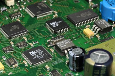
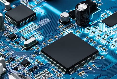
key technologies and progress in high-speed and high-density pcb design
High speed and high density have gradually become one of the significant development trends of many modern electronic products, and high speed and high density pcb design technology has become an important research filed.
Compared with traditional PCB design, high-speed and high-density PCB design has several key technical issues, which requires the development of new design technologies. There are also many theoretical and technical issues that need to be studied in depth. At the same time, the requirements for high-speed and high-density PCBs are getting higher and higher, which makes the design of high-speed and high-density PCB constantly face new problems; the continuous emergence of a large number of related research results has promoted the continuous development of high-speed and high-density PCB design technology. This article introduces the key technical issues (signal integrity, power integrity, EMC/EMI and thermal analysis) of high-speed and high-density PCB design and the new progress of related EDA technology, and discusses several important trends in high-speed and high-density PCB design.
Key technical issues
The key technical issues in high-speed and high-density PCB design mainly include signal integrity (SI), power integrity (PI), EMC/EMI and thermal analysis.
Signal Integrity
Signal integrity mainly refers to the quality of signal transmission on the signal line. When the circuit signal can reach the pin of the receiving chip with the required timing, duration and voltage amplitude, the circuit has good signal integrity. Signal integrity issues occur when the signal does not respond properly or the signal quality does not allow the system to operate stably over the long term. Signal integrity issues mainly include: delay, reflection, overshoot, ringing, crosstalk, timing, synchronous switching noise, EMI, etc.
Signal integrity issues will directly lead to signal distortion, timing errors, and erroneous data, address and control signals, causing system errors or even paralysis. Generally, for digital chips, a level above VIH is a logic 1, a level below VIH is a logic 0, and a level between VIL and VIH is an uncertain state. For digital signals with ringing, when the oscillation level enters the uncertain area of VIL ~ VIH, it may cause logical errors. The transmission of digital signals must have correct timing. General digital chips require that data must be stable before tsetup of the clock trigger edge to ensure correct logic timing. If the signal transmission delay is too long, the correct logic may not be received at the rising or falling edge of the clock, causing timing errors.
The causes of signal integrity problems are complex. Component parameters, PCB parameters, component layout on PCB, and high-speed signal routing are all important factors that affect signal integrity. Signal integrity is a system problem, and studying and solving signal integrity problems must be done from a system perspective.
Relatively speaking, people have been studying signal integrity issues for decades, have achieved many important theoretical and technical results, and accumulated rich experience. Many signal integrity technologies are relatively mature and have been widely used.
Power Integrity
Power integrity mainly refers to the fact that in high-speed systems, the impedance characteristics of the power distribution system (PDS) are different at different frequencies, which makes the voltage between the power layer and the ground layer on the PCB different at different places on the circuit board, thus causing The power supply is discontinuous, which generates power noise and causes the chip to not work properly. At the same time, due to high-frequency radiation, power integrity issues will also bring about EMC/EMI problems. In high-speed, low-voltage circuits, the harm of power supply noise is particularly serious.
The proposal of power integrity stems from the huge errors caused by performing signal integrity analysis based on wiring and device models without considering the influence of power supply.
Relatively speaking, the research on power integrity started late, and the theoretical research and technical means are not yet mature enough, which is one of the biggest challenges in the current high-speed and high-density PCB design. At present, some common measures are mainly taken to minimize the adverse effects caused by power integrity problems to a certain extent.
The main measures taken are: first, optimizing the stacking, layout and wiring design of the PCB; second, appropriately increasing the decoupling capacitor. When the system frequency is less than 300-400 MHz, placing appropriate capacitors in appropriate locations can help reduce the impact of power integrity issues. However, when the system frequency is higher, the effect of decoupling capacitors is small. In this case, the impact of power integrity issues can only be reduced by optimizing the PCB design.
EMC
EMC (electro-magnetic compatibility) is usually defined as: “the ability of a device or system to work normally in its electromagnetic environment and not cause unbearable electromagnetic disturbance to anything in the environment.” Some also define it as: “the study of the electromagnetic compatibility of a device or system in a limited environment.” It is a science that allows various electrical devices (subsystems, systems, and in a broad sense, organisms) to coexist without causing degradation under the conditions of limited space, limited time, and limited spectrum resources.
EMC mainly studies two aspects: EMI (electro-magnetic interference) and EMS (electro-magnetic susceptibility). EMI is generated when the electromagnetic interference source transfers energy to the sensitive system through the coupling path. It includes three basic forms: conduction through wires and common ground wires, radiation through space, or coupling through near fields.
EMC of electronic products is very important. Currently, many countries and regions have strict and complete EMC standards. More and more electronic products must pass relevant EMC testing and certification before entering the market. Moreover, as the electromagnetic environment deteriorates, the EMC requirements for electronic products will become increasingly higher.
Relatively speaking, EMC issues are the most complex. When the rise time or fall time is reduced from 5 ns to 2.5 ns, the EM I will increase by about 4 times. The spectrum width of EM I is inversely proportional to the rise time. The radiation intensity of EM I is proportional to the square of the frequency. The frequency range of this type of EM I radiation is about tens of MHz to several GHz. The wavelengths corresponding to these high frequencies are very short. Short connecting wires on the PCB or even the interconnects within the chip may become efficient transmitting or receiving antennas, thus causing serious EMC problems. Henry W Ott, president of Henry Ott Consulting, emphasized in his keynote speech at the PCB Design Conference-East: “In the era of high-speed design, PCB designers will face Many unexpected problems.” “EMC will become a greater challenge as designs get faster and wireless designs become more prevalent.”
Due to the complexity of EMC and the increasingly higher requirements of modern electronic products for EMC, EMC technology will be an important field that requires long-term research. At present, the prevention and solution of EMC problems mainly follows some common PCB design constraints, but the specific adoption of those rules and their effectiveness must be analyzed on a case-by-case basis, which depends largely on the theoretical level and practical experience of the designers.
Thermal Analysis
The dynamic power consumption of widely used CMOS digital chips increases with the increase of operating speed. For example, the dynamic power consumption Pdyn of CMOS inverter = CLV2DDf0→1. Due to the skin effect, the effective conductive cross-sectional area of the connecting wire decreases with the increase of frequency, causing the resistance of the connecting wire to increase with the increase of frequency (Rac∝ f).
The connecting wires also have inductance, and the inductive reactance (2πfL) also increases with increasing frequency. The impedance of the connecting wire can be considered as the series connection of the two.
It can be seen that the power consumption of the connecting wires also increases with the increase of working speed.
More power consumption means more heat. The high-density pin packaging and miniaturized packaging of components, as well as the increased density of components on PCBs, all make the heat dissipation conditions worse. These factors can cause the PCB temperature to be too high.
Electronic components have a specified operating temperature range. Increased temperature will cause component performance degradation and premature failure. Excessively high temperature will burn out components, PCB traces, vias, etc. Therefore, thermal analysis of high-speed and high-density PCBs is also very important. Through thermal analysis, the thermal field distribution of the PCB, the temperature of components and solder joints, and the potential heat dissipation and reliability problems in the PCB design can be determined so that necessary measures can be taken in a targeted manner.
Thermal analysis of high-speed and high-density PCBs involves many complex factors, such as heat transfer theory, thermal models of components, layout of components, circuit operation modes (such as static and dynamic), natural and artificial heat dissipation measures, etc., so this work is very complex. Difficult to accomplish manually. Although some EDA tools have thermal analysis functions, they are far from meeting the needs of high-speed and high-density PCB design.
By the way, it should be pointed out that issues such as signal integrity, power integrity, EMC/EM I in high-speed and high-density PCBs influence and restrict each other. During the PCB design process, these issues need to be considered comprehensively.
New progress in related EDA technologies
From the key technical issues of high-speed and high-density PCB, it can be seen that the traditional PCB design method can no longer meet the needs of high-speed and high-density PCB design. According to experts: “To carry out high-speed system design, we must first have a strong high-speed design concept and high-speed design Theory, standardized design process, use advanced high-speed design tools, conduct sufficient pre-analysis, obtain certain constraint rules, strictly follow the rules to drive layout and routing, strictly perform post-simulation verification to ensure the accuracy of the design, and repeatedly pass this design Process practice can continuously improve design skills in the field of high-speed design. “It can be seen that for high-speed and high-density PCB design, in addition to the necessary theoretical knowledge and practical experience, the help of advanced EDA tools is crucial. By using the simulation function of EDA tools, we can determine whether the function is correct and what the performance is like; we can determine whether the direction of improvement is correct and what the effect is; we can compare and select different solutions.
For high-speed and high-density PCB design, from schematic design to PCB design is generally completed with the help of EDA tools.
Currently popular EDA tools include Protel, PADS, OrCAD, Cadence, Mentor, etc. These EDA tools have their own characteristics, and their functions and usage can be found in many documents and websites. Some EDA tools support PCB simulation to varying degrees, including signal integrity simulation, electromagnetic interference simulation, thermal simulation, etc. Cadence, Mentor, etc. are more successful in PCB signal integrity and electromagnetic interference simulation; FLOTHERM, Auto Therm, BETAsoft, Quick Thermal, etc. are more successful in PCB thermal simulation. The following mainly introduces the new developments in these simulation functions.
For signal integrity simulation, Cadence’s SpectraQuest is a good simulation tool.
It can be used to perform modeling and simulation in the early stages of design, thereby forming constraint rules to guide later layout and routing and improve design efficiency. In June 2004, Cadence launched the MGH simulator specifically for 1000 MHz, which can complete the simulation of tens of thousands of BIT 1000 MHz signals in a few seconds, making the simulation function more powerful.
Because power integrity is a new challenge, relatively few simulation tools are available today.
It is reported that Cadence’s power integrity tool PI has been launched on the market and has been successfully applied to the designs of some customers.
Currently, the simulation effect of EMC/EM I is the worst, mainly due to the complexity of EMC/EM I. At present, the main method used is expert inspection, which converts EMC/EMI issues into layout and wiring rules on PCB according to international general standards. Cadence’s EMControl is such a rule checking tool similar to an expert system. It also provides a customized interface to facilitate customers to write EMC/EMI checking rules suitable for their own company. Mentor Graphics’ Quiet Expert can check incorrect wiring structures that cause EM I problems, identify the problems, and provide the causes and suggested solutions to the EM I problems. In terms of three-dimensional analysis, Ansoft, Ap sim, etc. can provide specialized tools and methods, and these tools can be used in conjunction with Cadence and Mentor Graphics system tools.
FLOTHERM is a standard thermal analysis software for the electronics industry.
It is a thermal analysis software based on computational fluid dynamics (CFD). Thousands of companies worldwide exchange thermal models with FLOTHERM. Leading electronic component manufacturers offer FLOTHERM models of their products to their customers.
Auto Therm board-level thermal analysis tool moves PCB thermal analysis to the early stage of the design process, achieving first-time success in PCB design and improving PCB reliability. Auto Therm automatically generates a complete thermal model from the LAYOUT or Fablink database, speeding up the thermal definition of the board, components and environment and reducing the execution time of thermal analysis. Analysis results can be customized in the form of graphs, charts and reports. Using the what-if analysis method, by changing boundary conditions, placing components, and adding heat sinks or fans, the board-level thermal distribution under different conditions can be quickly analyzed and proposed. Auto Therm can perform steady-state and transient conduction, convection, and radiation analysis to study transient effects of cooling failures and cycling processes.
BETAsoft can easily identify potential thermal and reliability issues in your design by determining the temperature of the PCB and its gradient, as well as the temperature of components and solder joints. Due to the use of local variable step-size finite element differential method, its calculation speed is greatly improved compared with the traditional finite element algorithm. BETAsoft can establish complex three-dimensional airflow and thermal field models for heat conduction, convection and radiation, and consider whether heat sinks, chip fans, thermal pads and other cooling devices are installed on the components. The error between BETAsoft’s analysis results and actual measurement results can be less than 10%.
Quick Thermal enables online real-time thermal analysis of PCB designs, and can quickly, flexibly and conveniently evaluate the thermal status of PCBs. It has flexible thermal analysis environment setting and component property setting functions to facilitate quick compromise. It has intuitive real-time isotherm result display, alarm display and other functions. In addition, Altium’s Protel 2004 also has significant enhancements in simulation capabilities.
Some development trends
Chip design, package design and PCB board-level design are inseparable
For the design process on silicon wafer, it is necessary to consider using a suitable package to match the PCB. The overall layout of the chip design is not only limited by the process, but also needs to take into account many constraints at the PCB board level. What should be considered.
There will be discontinuities in the signal where matching problems will occur.
For chip packaging, matching with PCB is one aspect, but more importantly, the appropriate packaging selection is very helpful in solving problems such as signal integrity, EMC/EM I at the PCB board level. For example, some timing issues that are difficult to solve on the PCB can be easily solved in the package. The new packaging design aims to reduce the parasitic parameters of the chip and thus weaken the parasitic effects. The parasitic effects of the chip include ground bounce and noise, propagation delay, edge rate, frequency response, output lead skew, antenna effect, etc. New package designs mainly include multiple ground and power pins, short leads, and a layout that minimizes capacitive coupling between pins. The new packaging design has a significant effect on improving EMC performance. For example, the DQFN package has a smaller lead frame and utilizes package solder terminals instead of external leads, greatly reducing the package connection wire length and related parasitic parameters. Compared with TSSOP package, the connection length of DQFN package is reduced by more than 50%.
Therefore, for high-speed and high-density PCB design, chip design, package design and PCB board-level design are becoming increasingly inseparable, requiring designers to consider the design of Silicon-Package-Board at the same time and coordinate the relationship between them. This is also a major problem that EDA manufacturers need to face in the long run.
Cadence is a leader in system-level process design. Its Allegro platform covers both board-level design and package-level design, and can be connected with several other chip design platforms of Cadence to form a complete design chain and realize effective data exchange. and communication. In addition, Cadence’s VSIC (virtual system interconnect) design method is a new Silicon-Package-Board collaborative design method that allows designers to consider the timing or signal integrity issues caused by the entire system in the early stages of design, solving thousands of A major challenge in MHz signal design.
The role of EDA tools is becoming increasingly important
On the one hand, as far as the key technical issues of high-speed and high-density PCB are concerned, the perfect solution of any one of them cannot be separated from the help of EDA tools. On the other hand, the increasingly higher requirements for high-speed and high-density PCBs have in turn prompted EDA manufacturers to continuously develop better EDA tools. The two form a virtuous circle and their relationship becomes increasingly close. It is certain that in high-speed and high-density PCB design, the role of EDA tools is becoming more and more important. For designers, timely mastering and appropriately applying advanced EDA tools will become one of the necessary qualities.
At present, EDA covers a wide range of fields, including networks, communications, computers, aerospace, etc.
The products involve system board-level design, system digital/intermediate frequency analog/mixed digital and analog/radio frequency simulation design, system IC/ASIC/FPGA design/simulation/verification, hardware and software collaborative design, etc. There are many manufacturers engaged in the research and development of EDA tools, the most representative of which are Cadence, Mentor Graphics, Synopsis, etc. Each manufacturer has its own strong products. In terms of market share, Cadence’s strong products are IC board design and services, MentorGraphics’ strong products are PCB design and deep submicron IC design verification and testing, and Synopsis’ strong product is logic synthesis. It is difficult for any manufacturer to provide the strongest design process to meet various design needs. Manufacturers use product standardization to solve this problem, that is, to allow designers to use the strengths of multiple companies in their design process to form the best design process.
Concurrent design will be widely used
As the competition in electronic products becomes increasingly fierce, it is very important to shorten the product design cycle as much as possible and bring the product to market as soon as possible. The recently introduced parallel design method is an important way to shorten the design cycle of large electronic systems. Concurrent design, also known as collaborative design, is to divide a large circuit board into several parts and have several people design it at the same time. At present, some parallel design tools can realize the connection and integration between various designs, can “see” the designs of other designers, and can even realize completely real-time parallel design. Mentor Graphics’ EDA tools have advantages in parallel design. The fully dynamic parallel design tool ExtremePCB launched at the end of 2004 is more powerful and can achieve fully real-time parallel design. Cadence’s concurrent design tools will also be available in the next version.
Conclusion
High speed and high density is one of the significant development trends of many electronic products. Research on high speed and high density PCB design technology has important practical significance. High-speed and high-density PCB design technology is very complex. It is restricted by the technical level of components, PCB boards, EMC, EDA, etc., and related research work is being vigorously promoted. New materials, new processes, new products, and new technologies are constantly emerging. , which makes high-speed and high-density PCB design constantly face new problems, and also promotes the continuous development of high-speed and high-density PCB design technology. The discussion in this article has a guiding role in the research and application of high-speed and high-density PCB design technology.